
Новини світу мікро- та наноелектроніки
My wife did 17.4K on Zoé
 | My wife groomed her and I thought of you guys and gals. [link] [comments] |
The art in a 1960's rack module
 | submitted by /u/1Davide [link] [comments] |
Change of guard at Intel Foundry, again

A little more than a year after he took the reins of Intel’s ambitious bid for semiconductor contract manufacturing, Stuart Pann is retiring while handing over the charge to Kevin O’Buckley. The transition took place on Monday, 13 May, and it once more raised questions about the future viability of Intel’s third-party foundry business.
Pann, a 35-year company veteran, joined Intel during the heydays of the PC revolution in 1981. He returned to the Santa-Clara, California-based semiconductor firm in 2021 to lead the chip manufacturing division, Intel Foundry Services (IFS). He replaced Intel Foundry’s first chief, Randhir Thakur, who later became CEO and managing director of Tata Electronics, the electronics manufacturing arm of Indian conglomerate Tata Group.

Figure 1 Pann, currently in a support role for a smooth transition, will retire at the end of this month. Source: Intel
Now O’Buckley replaces Pann, and it’s a déjà vu of Thakur-to-Pann handover a year ago. For instance, during the first quarter of 2024, Intel Foundry reported revenue of $4.4 billion, which was down by $462 million compared to the first quarter of 2023. That’s mainly attributed to lower revenues from back-end services and product samples.
Pann—who left the company only a few months after Intel Foundry marked the official launch of the manufacturing business as an independent entity to compete with the likes of TSMC and Samsung—set up Intel’s IDM 2.0 Acceleration Office (IAO) to guide the implementation of an internal foundry model. IAO closely works with Intel’s business units to support the company’s internal foundry model.
Intel Foundry, which aims to move beyond traditional foundry offerings and establish itself as the world’s first open-system foundry, faces huge technical and commercial challenges. That includes combining wafer fabrication, advanced process and packaging technology, chiplet standards, software, and assembly and test capabilities in a unified semiconductor ecosystem.
O’Buckley inherits these challenges. He comes from Marvell, where he led the company’s custom chips business as senior VP for the Custom, Compute and Storage Group. O’Buckley came to Marvell in 2019 via its acquisition of Avera Semiconductor, a 1,000-person chip design company that traces its roots to IBM, which offloaded it to GlobalFoundries before it was sold to Marvell. O’Buckley led Avera’s divestiture from GlobalFoundries.

Figure 2 Like his predecessor, O’Buckley will report directly to CEO Pat Gelsinger. Source: Intel
Intel CEO Pat Gelsinger, who has bet Intel’s revival bid on setting up an independent fab business, acknowledges that Intel Foundry is still some distance away from profitability due to the large up-front investment needed to ramp it up. However, time isn’t on Gelsinger’s side, meaning a swift turnaround plan is in order for O’Buckley.
O’Buckley is an outsider, a plus at Intel, where employees are known to have stayed long years; his expertise in the custom chips business will also be an asset at Intel Foundry. Next, during his stint at IBM, he spearheaded the company’s development of 22- and 14-nm FinFET technologies. As Gelsinger puts it, he has a unique blend of expertise in both foundry and fabless companies.
Now comes the tough part, execution.
Related Content
- Change of guards at Intel Foundry Services (IFS)
- Intel Signs MediaTek as Third Major Foundry Customer
- Intel Foundry’s ‘No. 1’ Customer—U.S. DoD—Targets GAA
- Intel Foundry Services roadmap unveiled one deal at a time
- Intel’s foundry foray and its influence on the EDA, IP industries
The post Change of guard at Intel Foundry, again appeared first on EDN.
Sampling and aliasing

If we want to take samples of some analog waveform, as in doing analog to digital conversions at some particular conversion rate, there is an absolute lower limit to the rate of doing conversions versus the highest frequency component of the analog signal. That limit must not be violated if the sampling process is to yield valid results. We do not want to encounter the phenomenon called “aliasing”.
The term “aliasing” as we use it here has nothing to do with spy thrillers or crime novels. Aliasing is an unwanted effect that can arise when some analog waveform is being sampled for its instantaneous values at regular time intervals that are longer than half the reciprocal of a sampling frequency. If we were to sample some waveform once every microsecond, the sampling interval is half of that one microsecond for which we would have a sampling frequency limit of 2 MHz or faster.
Aliasing will occur if the sampled waveform has frequency component(s) that are greater in frequency than 50% of the sampling frequency. To turn that statement around, aliasing will occur if the sampling frequency is too low. Aliasing will occur at any sampling rate that is lower than twice the highest frequency component of the waveform being sampled.
The next question is: Why?
The late comedian Professor Irwin Corey once posed a similar question: “Why is the sky blue?” His answer was something like “This is a question which must be taken in two parts. The first part is ‘Why?’ ‘Why’ is a question Man has asked since the beginning of time. Why? I don’t know. The second part is ‘Is the sky blue?’ The answer is ‘Yes!'”
Fortunately, we can do a little better than that as follows.
The sampling process can be thought of as multiplying the waveform being sampled by a very narrow duty cycle pulse waveform of zero value for most of the time and of unity value for the very narrow sampling time interval. That sampling waveform will be rich in harmonics. There will be a spectral line at the sampling frequency itself plus spectral lines at each of the sampling frequency’s harmonics as well. Each spectral line will have sidebands as shown in Figure 1 which will extend from those sampling frequency spectral lines up and down the frequency spectrum in keeping with the sampled waveform’s bandwidth.

Figure 1 Sampling versus aliasing where spectral line will have sidebands that will extend from those sampling frequency spectral lines up and down the frequency spectrum in keeping with the sampled waveform’s bandwidth.
The sampling waveform is amplitude modulated by the sampled waveform and so I’ve chosen to call that sampled waveform’s highest frequency component, Fmod. Each bandwidth is 2 * Fmod.
If the sampling frequency is high enough as with Fs1, the illustrated sidebands do not overlap. There is a respectable guard band between them, and no aliasing occurs.
If the sampling frequency starts getting lower as with Fs2, the sidebands start getting closer together and there is a less comfortable, if I may use that word, guard band.
If the sampling frequency gets too low as with Fs3 which is less than twice Fmod, the sidebands overlap, and we have aliasing. Sampling integrity is lost. The sampled waveform cannot be reconstructed from the undersampled output of this now unsatisfactory system.
Consider this an homage to Claude Shannon (April 30, 1916 – February 24, 2001) and his sampling theory.
John Dunn is an electronics consultant, and a graduate of The Polytechnic Institute of Brooklyn (BSEE) and of New York University (MSEE).
Related Content
- Digital oscilloscopes: When things go wrong
- The alias theorems: practical undersampling for expert engineers
- Control the sample rate of digitized signals
- Basics of ADCs and DACs, part 1
- Claude Shannon, ‘father of information theory,’ is born, April 30, 1916
The post Sampling and aliasing appeared first on EDN.
UK–APAC Tech Growth Programme report highlights opportunities in Taiwan
EPIR orders second Riber MBE 32 MCT research system
EPC presenting power solutions for automotive, robotics, power tools, solar at PCIM Europe
Semiconductor Mega Trends and Career Opportunities
The semiconductor industry is experiencing a profound transformation, propelled by technological advancements, market dynamics, and global initiatives. In India, this transformation is particularly significant, as the nation emerges as a key player in the semiconductor landscape. Let’s delve into the mega trends shaping the semiconductor industry in 2024, the career opportunities they present, and the role of the Electronics Sector Skills Council of India (ESSCI) in preparing professionals for this dynamic field.
Semiconductor Applications Across Diverse Fields:
Semiconductor chips serve as the fundamental building blocks powering a vast array of applications, wielding control over power management, enabling intricate power electronics systems, and orchestrating indispensable functions within electronic devices. From the ubiquitous smartphones and computers to the intricate network of IoT devices, semiconductor chips form the backbone, fuelling innovation and driving the seamless integration of technology into our daily lives.
- Driving Automotive Innovation: Semiconductor technology has spearheaded transformative advancements in the automotive sector, ushering in a new era of intelligent and dependable vehicles. By seamlessly integrating semiconductor components, automobiles have evolved to possess heightened intelligence, unparalleled reliability, and superior performance. Advanced Driver Assistance Systems (ADAS) rely on semiconductor solutions for critical features such as collision avoidance, lane departure warning, and adaptive cruise control.
- Revolutionizing Telecommunications: Semiconductor innovation is at the forefront of transforming the telecommunications landscape. With the emergence of 5G networks, semiconductor solutions are crucial for powering base stations, antennas, and network infrastructure, enabling faster data speeds, lower latency, and unparalleled connectivity. In addition to network infrastructure, semiconductor chips are integral to the development of smartphones, enabling advanced features such as AI-driven cameras, augmented reality, and facial recognition.
- Empowering Healthcare Technologies: Semiconductor technology is revolutionizing healthcare by driving advancements in medical diagnostics and patient care. Medical imaging devices, including MRI and CT scanners, heavily rely on semiconductor components for signal processing and image reconstruction, enabling precise diagnostics and treatment planning. Semiconductor chips also power medical monitoring devices such as wearable fitness trackers and smart health monitors, allowing for continuous health tracking and remote patient monitoring.
- Transforming Hearables and Wearables: The integration of semiconductor technology has led to remarkable advancements in hearable and wearable devices, revolutionizing the way we interact with technology. Hearables, such as wireless earbuds and smart headphones, leverage semiconductor chips for Bluetooth connectivity, noise cancellation, and audio processing, delivering immersive audio experiences. Similarly, wearable devices, including smartwatches and fitness trackers, rely on semiconductor solutions for sensors, data processing, and connectivity, enabling seamless health and activity tracking.
Career Opportunities in Semiconductor Technology:
As the semiconductor industry evolves in response to these mega trends, it creates exciting career opportunities for professionals across the value chain – designing, fabrication and packaging. From semiconductor design and manufacturing to research and development, there is a growing demand for skilled professionals who can innovate and drive technological advancements in the industry. The sector is expected to see more than 800,000 to 1 million job openings over the next five years, says staffing company Randstad. The government recently approved $15 billion worth of investments into the sector including from the Tata group. India’s burgeoning semiconductor sector is facing a surge in demand for talent, fuelled by new investments and the government’s ambitious plan to transform the country into a chip manufacturing hub.
- Semiconductor Design Engineer: Semiconductor design engineers play a crucial role in developing the architecture and circuitry of semiconductor chips. They utilize tools like Electronic Design Automation (EDA) software and simulation tools to design and optimize chip layouts for performance, power efficiency, and manufacturability.
- Process Engineer: Process engineers are responsible for developing and optimizing semiconductor manufacturing processes. They work closely with equipment vendors and manufacturing teams to ensure the smooth operation of semiconductor fabrication facilities, improve yield rates, and reduce production costs.
- Research Scientist: Research scientists in the semiconductor industry focus on exploring new materials, devices, and technologies to push the boundaries of semiconductor innovation. They conduct experiments, analyse data, and collaborate with cross-functional teams to develop next-generation semiconductor solutions.
- Material Engineers – Material engineers in the semiconductor industry are pivotal in researching, selecting, and optimizing the materials used in semiconductor device fabrication. Their expertise spans a wide range of materials, including silicon, gallium arsenide, and various compound semiconductors. Material engineers work closely with semiconductor design teams to ensure that the chosen materials meet the performance requirements of the intended applications while also considering factors such as cost, scalability, and reliability.
- Product Marketing Manager: Product marketing managers play a vital role in bringing semiconductor products to market. They conduct market research, develop marketing strategies, and collaborate with sales teams to promote semiconductor products and drive revenue growth.
- Quality Assurance Engineer: Quality assurance engineers ensure that semiconductor products meet the highest standards of quality and reliability. They develop and implement test plans, conduct performance testing, and analyse data to identify and address any issues or defects in semiconductor products.
- Packaging experts: Packaging experts in the semiconductor industry are instrumental in developing and implementing packaging solutions that safeguard semiconductor chips. Their role entails meticulous selection of packaging materials, designing efficient packaging structures to ensure protection against environmental factors and mechanical stresses, and optimizing designs for thermal management and electrical performance. They collaborate closely with design and manufacturing teams to ensure that packaging solutions meet stringent industry standards while balancing factors such as cost-effectiveness and manufacturability.
- Machine maintenance technicians –Machine maintenance technicians also play a crucial role in implementing preventive maintenance schedules, identifying opportunities for equipment upgrades or optimizations, and ensuring compliance with safety regulations and operational standards. Their expertise contributes to the overall efficiency and longevity of semiconductor manufacturing operations.
- Safety protocol checkers – These people are integral to maintaining a safe and secure work environment within semiconductor manufacturing facilities. They are responsible for enforcing safety regulations, conducting regular inspections to identify potential hazards, and implementing corrective measures to mitigate risks and prevent accidents. Safety protocol checkers also play a vital role in developing and implementing safety training programs, conducting safety audits, and promoting a culture of safety awareness among employees. Their diligence and vigilance help to safeguard the well-being of personnel, protect semiconductor manufacturing equipment, and maintain the integrity of semiconductor processes.
Qualifications: National Occupational Standards by ESSCI
As the field becomes more specialized, advanced degrees or skill training provide a competitive edge. Specialized qualifications like IC Package, VLSI Design, and Package Design enhance a designer’s expertise. As on date ESSCI has developed 25 NSQF aligned and approved qualifications on semiconductors (Design, Packaging & Manufacturing segment) and is also planning to develop more qualifications as per the need & demand of the industry especially on the Clean Room, Machine Maintenance and other related fragments, which are the need of the hour.
Short Term Qualifications & Upskilling NOS’s
ESSCI offers focused a range of qualifications covering the complete value chain of the semiconductor industry. Short Term courses such as VLSI Design Engineer, concentrating on designing SOC-module functions using software, Embedded Full Stack Engineer, IoT Hardware Analyst are some of the top courses offered for pursuing engineering graduates to gain the knowledge of EDA Tools and system design. ESSCI also provides qualifications for Wafer Back Grinding Engineer and Wafer Dicing Engineer, specialising in wafer manufacturing tasks which can be taught to ITI / Diploma students.
ESSCI also has foundation / upskilling courses in the field of Nano Science & Advance Nano Science which is also in great demand.
Also, there are some basic courses on the Industrial Safety – Electrical & Hazchem which are very crucial & important for the industrial safety requirements. The complete list of our qualifications along with their model curriculum are all uploaded on our website – https://essc-india.org/qualification-packs.php In conclusion, the semiconductor mega trends present unprecedented opportunities for India to assert its leadership in the global semiconductor industry. Through strategic investments, policy support, and talent development initiatives, India is poised to capitalize on these trends, driving innovation, fostering entrepreneurship, and creating a thriving semiconductor ecosystem for generations to come.
 Dr. Abhilasha Gaur, Chief Operating Officer
Electronics Sector Skills Council of India
The post Semiconductor Mega Trends and Career Opportunities appeared first on ELE Times.
Vishay Intertechnology 600 V E Series Power MOSFET in Compact Top-Side Cooling PowerPAK® 8 x 8LR Delivers Industry’s Lowest RDS(ON)*Qg FOM
Fourth-Generation Device Enables Higher Power Ratings and Density Versus D²PAK While Lowering Conduction and Switching Losses to Increase Efficiency
To provide higher efficiency and power density for telecom, industrial, and computing applications, Vishay Intertechnology, Inc. today introduced its first fourth-generation 600 V E Series power MOSFET in the new PowerPAK 8 x 8LR package. Compared to previous-generation devices, the Vishay Siliconix n- channel SiHR080N60E slashes on-resistance by 27 % and resistance times gate charge, a key figure of merit (FOM) for 600 V MOSFETs used in power conversion applications, by 60 % while providing higher current in a smaller footprint than devices in the D²PAK package.
Vishay offers a broad line of MOSFET technologies that support all stages of the power conversion process, from high voltage inputs to the low voltage outputs required to power the latest high tech equipment. With the SiHR080N60E and other devices in the fourth-generation 600 V E Series family, the company is addressing the need for efficiency and power density improvements in two of the first stages of the power system architecture — power factor correction (PFC) and subsequent DC/DC converter blocks. Typical applications will include servers, edge computing, super computers, and data storage; UPS; high intensity discharge (HID) lamps and fluorescent ballast lighting; telecom SMPS; solar inverters; welding equipment; induction heating; motor drives; and battery chargers.
Measuring 10.42 mm by 8 mm by 1.65 mm, the SiHR080N60E’s compact PowerPAK 8 x 8LR package features a 50.8 % smaller footprint than the D²PAK while offering a 66 % lower height. Due to its top-side cooling, the package delivers excellent thermal capability, with an extremely low junction to case (drain) thermal resistance of 0.25 °C/W. This allows for 46 % higher current than the D²PAK at the same on-resistance level, enabling dramatically higher power density. In addition, the package’s gullwing leads provide excellent temperature cycle capability.
Built on Vishay’s latest energy-efficient E Series superjunction technology, the SiHR080N60E features low typical on-resistance of 0.074 Ω at 10 V and ultra low gate charge down to 42 nC. The resulting FOM is an industry-low 3.1 Ω*nC, which translates into reduced conduction and switching losses to save energy and increase efficiency in power systems > 2 kW. For improved switching performance in hard-switched topologies such as PFC, half-bridge, and two-switch forward designs, the MOSFET released today provides low typical effective output capacitances Co(er) and Co(tr) of 79 pF and 499 pF, respectively. The package also provides a Kelvin connection for improved switching efficiency.
The device is RoHS-compliant and halogen-free, and it is designed to withstand overvoltage transients in avalanche mode with guaranteed limits through 100 % UIS testing.
Samples and production quantities of the SiHR080N60E are available now. For lead time information, please contact your local sales office.
The post Vishay Intertechnology 600 V E Series Power MOSFET in Compact Top-Side Cooling PowerPAK® 8 x 8LR Delivers Industry’s Lowest RDS(ON)*Qg FOM appeared first on ELE Times.
Optimize IoT Device Battery Life with Emulation and Profiling Software
Internet of things (IoT) devices have many uses in consumer, medical, and industrial areas. With more IoT devices coming to market, battery duration becomes essential for product quality and customer satisfaction. Their safety depends on battery performance for many of these applications, such as implantable medical devices. When the expected battery life does not meet real-world requirements, the device can become very dangerous for patients.
Battery life requirements are also high for intelligent city or asset-tracking applications. A smart meter in every home or a small asset tracker in every item will need a long-lasting battery, as changing batteries over a large deployment area is not profitable. Therefore, testing and predicting a device’s battery life is more important than ever.
With battery emulation and profiling software, device designers can estimate battery life precisely. Moreover, emulation software can evaluate current drain to modify device designs that can extend battery duration.
Importance of battery profiling softwareBatteries are nonideal energy sources because they interact with the device, influencing the current drain of the battery. Precise current consumption results are crucial for maximizing a device’s battery life. Consider the battery’s features when using a DC source to power the device to ensure that the current consumption results correctly imitate the battery current consumption.
There are several reasons why battery profiling and characterization are essential. Users must know how much energy the battery can hold and deliver as it drains over time. The open circuit voltage (VOC) and internal resistance (IR) change as the battery drains. These need to be plotted so that the battery profiles show the actual performance of the battery in the real world. Figure 1 shows a typical plot example of a battery profile.
Verifying the battery’s performance under certain discharge conditions and operating modes is also essential. Factors that influence battery behavior are:
- Temperature
- Load current profiles (constant/dynamic)
- Different operating modes, including constant current, power, and resistance
Battery life depends on these parameters, so making different battery profiles that suit specific discharge situations is essential.
A general-purpose DC source aims to be a perfect voltage source with no output impedance by using remote sensing feedback to maintain its output voltage constant. However, unlike a battery, its voltage does not decrease with load current. Moreover, feedback regulation is not instantaneous, which causes voltage drop and overshoot when loading and unloading changes. A significant transient voltage drop can activate a device’s low-battery-voltage shutdown.
When powering a device with a DC source, emulate the battery’s characteristics for current drain results comparable to those of a battery. A regular DC source differs from a battery, but a DC source that can imitate a battery helps users get more reliable results. Make sure the power supply used has a programmable output resistance.
Extending battery life with emulation softwareUsing a battery emulator instead of a battery has several advantages for device testing:
- Creates a safer test environment: By using an emulator, designers do not have to physically charge and discharge batteries, which can become dangerous with repeated cycles.
- Achieves repeatable results: Characteristics of an emulated battery do not vary from physical batteries, whose characteristics can fluctuate after charging / discharging. They can also vary between different batteries, even in the same model.
- Reduces test setup times: Designers can instantly simulate any state of charge (SoC) versus manually draining a battery to the desired level to speed testing.
A battery emulator operates through several steps. The initial step is to load a battery profile. This profile is the data from a graph of the battery voltage and internal resistance against the SoC, as shown in Figure 1. Designers can generate a battery profile using battery modeling software or get a profile from a battery provider.
Creating a profile with modeling software will make the profile match the current consumption for a particular device, which is more precise than a generic profile from a battery supplier. For instance, a generic profile is not helpful if the battery supplier makes the profile based on a steady current draw when the device under test has a variable current consumption. Figure 2 shows a battery profiler with a current consumption profile from a device loaded into it. The software repeats the waveform until the battery runs out of power.
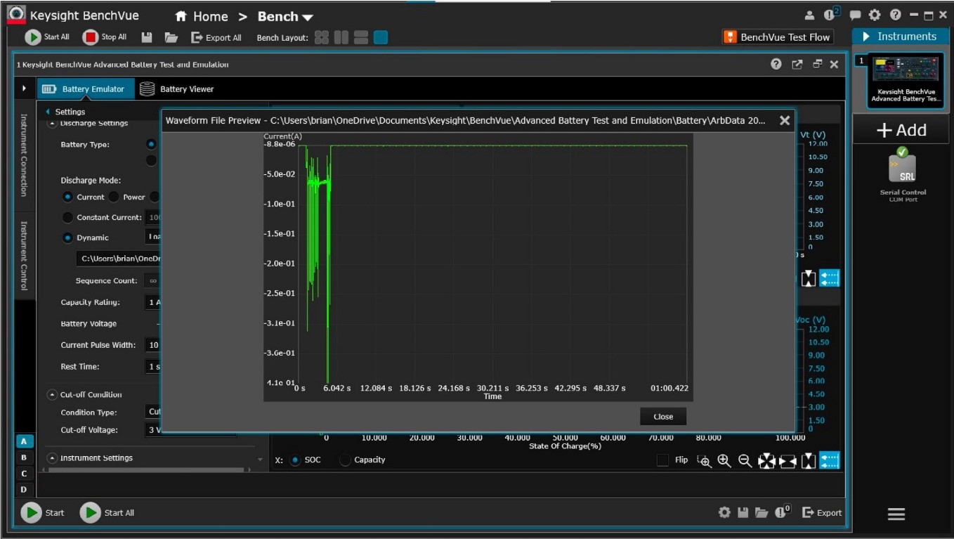 Figure 2. Example of a device’s current consumption waveform loaded into an advanced battery test and emulation software.
The next step is to choose the initial SoC and the termination voltage. Designers will link the device to the emulator and begin the battery emulation with software. Battery emulators constantly monitor the current, whether charging or discharging, to dynamically compute the emulated SoC. The emulator continually adjusts its output (voltage and resistance) according to the SoC to match the loaded battery profile. The test finishes when the emulator reaches the termination voltage if the emulator discharges.
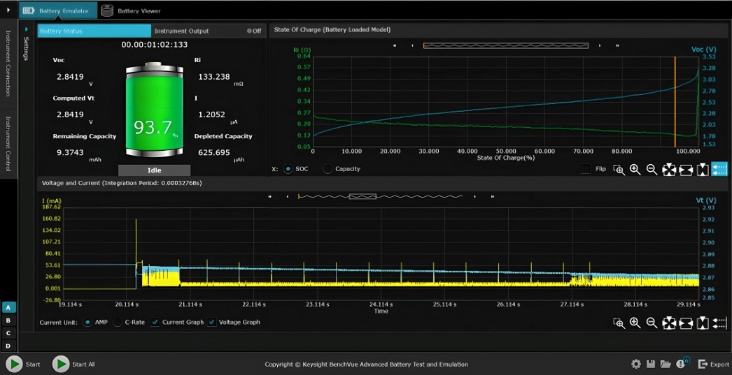 Figure 3. Example of a device’s battery emulation using advanced battery test and emulation software.
Designers can learn more about a device’s behavior by quickly emulating a battery at various SoCs. Figure 4 shows the information engineers can obtain from a device’s current drain. Engineers can use the data from this analysis to modify the design of the IoT device to improve battery performance.
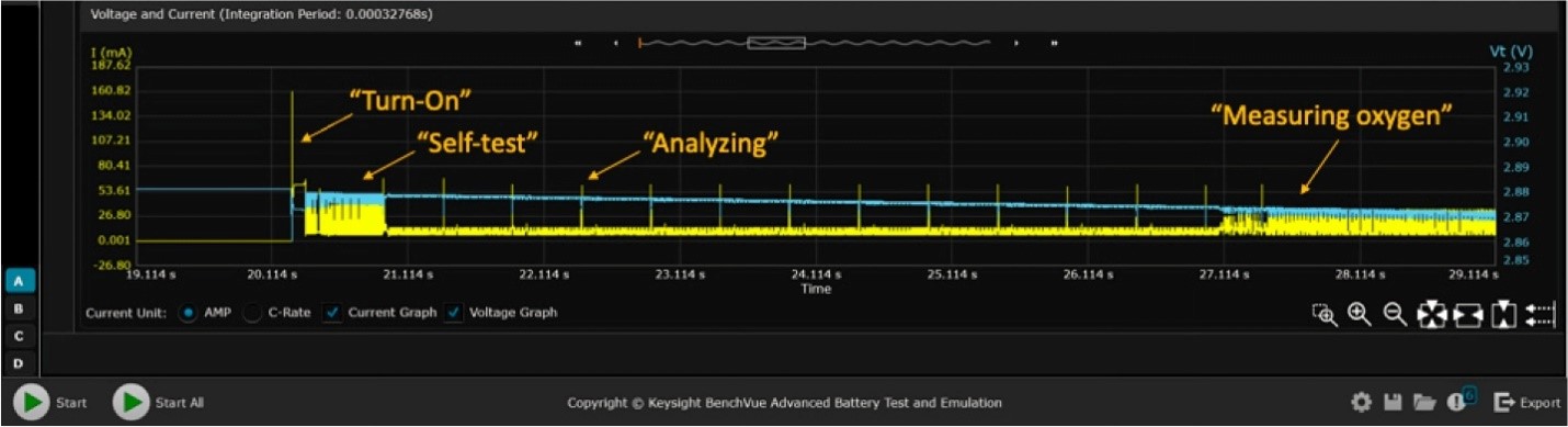 Figure 4. Current drain analysis of a pulse oximeter medical IoT device using advanced battery test and emulation software.
Cycling battery charge/ discharge to determine capacity loss
Figure 4. Current drain analysis of a pulse oximeter medical IoT device using advanced battery test and emulation software.
Cycling battery charge/ discharge to determine capacity loss
Engineers need to know the energy a battery can store and deliver to IoT devices. Battery test and emulation software helps visually monitor battery charging and discharging to measure capacity. Software must support constant current (CC) and voltage (CV) modes for charging batteries. When the battery is nearly full using CC mode, the software must switch from CC mode to a mix of CC and CV. This mix is needed because a battery cannot be charged at the same rate when it reaches maximum voltage or capacity.
It is also crucial for the software to support constant current, constant resistance, and continuous power modes when discharging a battery. Engineers can use software to test and emulate current consumption profiles directly from a device. This feature allows engineers to quickly discharge the battery with a profile matching the current drain during usage. Running it throughout the rundown test and simulating it using the actual device to analyze the battery drain is simpler.
Battery performance can deteriorate significantly over a lifetime of charging and discharging. That is why it is essential to simulate battery cycling. Battery test and emulation software is a convenient solution, but the software must support data logging. Also, generating different charging and discharging profiles for a battery is very useful in a battery test and emulation software solution.
Designers can mix various charging and discharging sequences to simulate complex charging and discharging cycling profiles. Then, they can measure how a battery’s performance declines over time. Emulation software solutions are ideal for this as they can enable, for example, up to one thousand cycle operations to assess the battery’s aging effect and reliability under sequence test conditions.
SummaryBattery profiling and emulation software are essential for IoT device power analysis. They help improve battery life, mimic any charge and battery profile state, create more reliable and consistent test environments, and measure capacity loss and aging effects. This is important for product quality, customer satisfaction, and safety in various consumer, medical, and industrial applications.
The software ensures engineers do not have to charge and discharge batteries, which can become dangerous with repeated cycles—instantly simulating any state of charge versus manually draining a battery to the desired level. Battery software helps create a safer test environment, measures accurate, repeatable results, and reduces test setup times.
 Andrew Herrera, Product Marketing Manager – Keysight Technologies
The post Optimize IoT Device Battery Life with Emulation and Profiling Software appeared first on ELE Times.
Research explores the effects of nuclear magnetic resonance on internal clock of cells
Wolfspeed quarterly revenue hit by weak industrial and energy markets
Cancel thermal airflow sensor PSRR with just two resistors

Self-heated transistors used as thermal air flow sensors are a particular (obsessive?) interest of mine, and over the years I must have designed dozens of variations on this theme. Figure 1 illustrates one such topology seen here before. It connects two transistors in a Darlington pair with Q2 serving as an unheated ambient thermometer and Q1 as the self-heated airflow sensor. Reference amplifier A1 and current sense resistor R3 regulate a constant 67 mA = heating current = 333 mW @ 5 V heating power.

Figure 1 Typical self-heated transistor thermal airflow sensor.
Wow the engineering world with your unique design: Design Ideas Submission Guide
This heat input raises Q1’s temperature above ambient by 64oC at 0 fpm air speed, cooling to 24oC at 1000 fpm as shown in Figure 2.

Figure 2 Thermal sensor temperature versus air speed.
As shown in Figure 2, the relationship between the airspeed and cooling of the self-heated transistor sensor is highly nonlinear. This is an inherent characteristic of such sensors and causes the sensor temperature versus air speed signal to be equally nonlinear. Consequently, even relatively small power supply instabilities, that translate % for % into instability in sensor temperature rise, can create surprisingly large airspeed measurement errors.
Clearly, anything less than perfect power supply stability can make this a problem.
But Figure 3 offers a surprisingly simple and inexpensive fix consisting of just two added resistors: R7 and R8.

Figure 3 Added R7 and R8 establish an instability-cancelling relationship between heating voltage V and heating current I.
The added Rs sum feedback from current sensing R3 with heating voltage source V. Summation happens in a ratio such that a percentage increase in V produces an equal and opposite percentage decrease in current I, and vice versa. The result is shown graphically in Figure 4.
Note the null (inflection) point at 5 V where heating is perfectly independent of voltage.

Figure 4: Sensor temperature versus supply voltage where: Blue = heating voltage V and (uncorrected) power; Red = heating current I; and Black = I*V = heating power / temperature.
Here’s the same thing in simple nullification math:
I = (0.2 – V*R8/R7)/R3 = (0.2 – 0.02V)/R3
H = I*V = (0.2V – 0.02V2)/R3
dH/dV = (0.2 – 0.04V)/R3 = (0.2 – 0.2)/R3 = 0 @ V = 5 volts
dH = -0.01% @ V = 5 volts ±1%
Note the 200:1 stability improvement that attenuates a ±1% variation in V down to only -0.01% variation in heating power and therefore temperature.
Problem solved. Cheaply!
Stephen Woodward’s relationship with EDN’s DI column goes back quite a long way. Over 100 submissions have been accepted since his first contribution back in 1974.
Related Content
- Self-heated Darlington transistor pair comprises new air flow sensor
- Nonlinearities of Darlington airflow sensor and VFC compensate each other
- Adding one resistor improves anemometer analog linearity to better than +/-0.5%
- Transistor linearly digitizes airflow
- A groovy apparatus for calibrating miniature high sensitivity anemometers
- 1kHz per Kelvin temperature sensor
The post Cancel thermal airflow sensor PSRR with just two resistors appeared first on EDN.
Is Rohm closer to acquiring Toshiba’s power chip business?

As Rohm Semiconductor deepens its ties with Toshiba Electronic Devices & Storage, industry watchers wonder if Rohm is getting closer to acquiring Toshiba’s power chips business. It all began late last year when the two companies announced a joint investment of $2.7 billion to collaborate on manufacturing power electronics devices.
But what made this news more noteworthy was that the announcement followed Rohm’s becoming part of a private equity group that was planning to take Toshiba private. However, when the two companies joined hands to boost the volume production of power devices, they stated that they had been considering this collaboration for some time and that it wasn’t a starting point in Rohm acquiring Toshiba’s power semiconductors business.
There is a third player in this $2.7 billion investment plan: the Japanese government, which adds another dimension to this hookup between Rohm and Toshiba Electronic Devices & Storage. Japan, aiming to strengthen the resilience of its semiconductor supply chains, recognises the strategic importance of power electronics and wants to double the power chip production in the country.
Moreover, Japan sees the local power chip industry as too fragmented, which makes it hard for them to compete with companies like Infineon. So, the Japanese government will subsidize one-third of this $2.7 billion investment in power semiconductor production on part of Rohm and Toshiba.
A closer look at this dimension also adds merits to the possibility of Rohm subsequently acquiring Toshiba’s power semiconductors business. It’s worth mentioning that Rohm was the first company to mass produce silicon carbide (SiC) MOSFETs, and it’s been continuously investing in this wideband gap (WBG) technology since then.

Figure 1 The Miyazaki Plant No. 2, based on assets acquired from Solar Frontier in July 2023, is dedicated to manufacturing SiC power devices. Source: Rohm
In the $2.7 billion joint investment plan announced late last year, Rohm will invest ¥289.2 billion in its new plant in Kunitomi, Miyazaki Prefecture, to produce SiC power chips. Toshiba will invest ¥99.1 billion in its newly built 300-mm fab in Nomi, Ishikawa Prefecture, to produce silicon-based power chips.
After delisting late last year, Toshiba faces an uncertain future. However, it still possesses highly valuable assets, and its power electronics business is one of them. There has also been chatter about splitting Toshiba into three units.

Figure 2 Vehicle electrification and automation of industrial equipment have led to strong demand for power devices like MOSFETs and IGBTs at 300-mm fab in Nomi. Source: Toshiba
When you see this potential divesture in the wake Japan’s desire to have a power electronics company that can compete with the likes of Infineon, Rohm taking over Toshiba’s power semiconductors business seems like a no-brainer. Among Japan’s current power chip firms, Rohm is known to have a stable power electronics business.
And the company is keen to affirm its management vision: “We focus on power and analog solutions and solve social problems by contributing to our customers’ needs for energy savings and miniaturization of their products.” Given this backdrop, Rohm taking over Toshiba Electronic Devices & Storage is probably a matter of time.
Related Content
- Toshiba is at crossroads, again
- New Rohm Fab Will Add Capacity for SiC Devices
- Zhenghai Group, Rohm Form JV for SiC Innovations
- Toshiba to spin off San Jose MPU engineering division
- Toshiba’s moment of semiconductor truth nears with upcoming split
The post Is Rohm closer to acquiring Toshiba’s power chip business? appeared first on EDN.
Waaree Renewable Technologies Limited Q4 results FY24
- Record Year of Strong Growth
- Record Revenue growth of 149.73% YoY at Rs. 876.44 crores and Record PAT growth of 167.55% YoY at Rs. 148.04 crores
- Unexecuted Orderbook of 2,365 MWp to be executed in next 18 months
Waaree Renewable Technologies Limited, the Solar EPC subsidiary of Waaree Group, a solar developer that finances, constructs, owns and operates solar projects, has reported its audited financial results for the quarter and nine month ended March 31, 2024.
KEY PERFORMANCE HIGHLIGHTS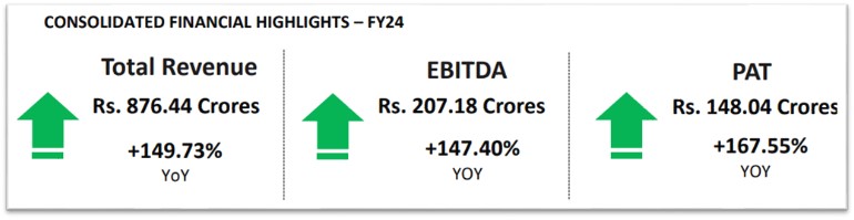
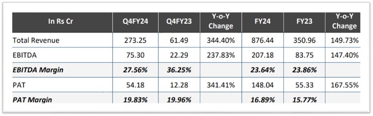
FY24
- Revenue for FY24 stood at Rs. 876.44 crores representing a growth of 149.73% YoY as compared to Rs.350.96 crores in FY23
- EBITDA for FY24 stood at Rs. 207.18 crores as compared to Rs. 83.75 crores in FY23 representing a growth of 147.40% YoY
- PAT for FY24 stood at Rs. 148.04 crores as compared to Rs. 55.33 crores in FY23 representing a growth of 167.55% YoY
Q4FY24
- Revenue for Q4FY24 stood at Rs. 273.25 crores representing a growth of 344.40% YoY as compared to Rs. 61.49 crores in Q4FY23
- EBITDA for Q4FY24 stood at Rs. 75.30 crores as compared to Rs. 22.29 crores in Q4FY23 representing a growth of 237.83% YoY
- PAT for Q4FY24 stood at Rs. 54.18 crores as compared to Rs. 12.28 crores in Q4FY23 representing a growth of 341.41% YoY
Order book Position:
- Unexecuted order book stands at 2,365 MWp
- Bidding pipeline remains robust
Key Updates:
- The Company has successfully completed the corporate action of a stock split, reducing the face value of its Equity shares in the ratio of 1:5 per share. The face value of shares now stands at Rs. 2/- per share
- Recent Order Wins
- 980 MWp Ground Mounted solar power project
- 412 MWp Ground Mounted solar power project
- 450 MWp Ground Mounted Solar power Project
- 4 MWp Ground Mounted solar power project
Commenting on the results Mr. Dilip Panjwani, CFO, Waaree Renewable Technologies Limited said: “As a company committed to driving sustainable solutions, we are excited to share our progress and the significant opportunities that lie ahead. India has set an ambitious target to reduce the carbon intensity of the nation’s economy by less than 45% by the end of the decade, achieve 50 percent cumulative electric power installed by 2030 from renewables, and achieve net-zero carbon emissions by 2070. The country aims for 500 GW of renewable energy installed capacity by 2030.
The country’s renewable energy market is on the rise, with a record 69GW of bids in FY2024, surpassing the government’s target. Solar power, both grid-scale and rooftop, remains the primary contributor, accounting for 81% of the added capacity. The installed solar energy capacity has increased by 30 times in the last 9 years and stands at 81.81 GW as of March 2024.
Policy initiatives like the PM Surya Ghar: Muft Bijli Yojana aim to further boost solar installations, particularly in residential areas. With a strong balance sheet and disciplined financial management, the focus is on executing profitable projects with higher returns. This progress signifies not only environmental strides but also promising economic prospects in India’s renewable energy landscape.
We are also pleased to inform you that the board of directors has recommended a dividend of Rs. 1/- for the face value of share of Rs. 2/- each. With a sound balance sheet and disciplined capital management, we are well-equipped for the next phase of growth. We also would like to extend our gratitude to stakeholders for their continued trust and support.”
The post Waaree Renewable Technologies Limited Q4 results FY24 appeared first on ELE Times.
I built a WS2812 flower
 | My first attempt at something freeform. A couple of WS2812 controlled by a small esp32 board. The feet are connected to capacitive touch sensors to control on/off, color mode and brightness. [link] [comments] |
Broken UHF Radio
 | Ear piece no longer works on my radio after I went to the ground and landed on it causing the metal ring to come out. Radio still works fine just not with an ear piece. What would I have to do to go about fixing this? [link] [comments] |
Weekly discussion, complaint, and rant thread
Open to anything, including discussions, complaints, and rants.
Sub rules do not apply, so don't bother reporting incivility, off-topic, or spam.
Reddit-wide rules do apply.
To see the newest posts, sort the comments by "new" (instead of "best" or "top").
[link] [comments]
EEVblog 1614 - Circuit Design TIP: Crystal Oscillators
CSconnected appoints Howard Rupprecht as new managing director
Сторінки


![[link]](https://i.redd.it/0p8dhstf0f0d1.jpeg)