
ELE Times

New Plug-In Timing Module Delivers Precise, Reliable Synchronization for Data Centers and 5G Networks to Meet the Demands of AI and Next-Generation Connectivity
National, 24th April 2026: As data centers and 5G networks become the backbone of AI-driven innovation and digital transformation, the need for precise, resilient timing solutions has never been more critical. Timing is not just a technical requirement, but rather a strategic enabler for high-performance, scalable infrastructure. Microchip Technology (Nasdaq: MCHP) today announces its MD-990-0011-B family of plug-in timing modules, delivering turnkey, high-precision synchronization for data center servers and 5G virtualized Radio Access Networks (vRAN).
Developed in collaboration with Intel, the MD-990-0011-B timing module is designed for seamless compatibility with Intel® Xeon® 6 SoC-powered server platforms, supporting both OEMs and ODMs in building future-ready systems. By leveraging Intel’s foundational vRAN architecture, the module enables robust, low-latency time synchronization, which is essential for distributed AI workloads and real-time applications.
Engineered for the reliability and scalability required by cloud infrastructure, virtualization, and high-availability deployments, the MD-990-0011-B supports automatic source selection and locking across Global Navigation Satellite Systems (GNSS), Synchronous Ethernet (SyncE), and Precision Time Protocol (PTP). This flexibility supports continuous, accurate timing even as network demands evolve.
“Timing is the invisible force that guides the world’s most transformative technologies. With the MD-990-0011-B timing modules, Microchip enables designers to address timing requirements proactively, whether at the outset or during upgrades,” said Randy Brudzinski, corporate vice president of Microchip’s frequency and time systems business unit. “Our plug-in solution eliminates the complexity of custom timing circuits, providing integration and reliability, accelerating innovation and reducing time-to-market for data centers and 5G networks.”
“Microchip’s MD-990-0011-B Timing Module aligns with Intel’s commitment to enable next-generation infrastructure by providing scalable, high-performance platforms that are ready for the demands of 5G, AI and cloud computing,” said Mike Merluzzi, GM of radio access networks at Intel Corporation. “By simplifying timing integration and enhancing reliability on Intel Xeon 6 SoC-powered platforms, we’re helping customers accelerate innovation and deployment.”
Delivering exceptional precision in time and frequency accuracy, along with robust holdover capabilities, the MD-990-0011-B timing modules are available in two variants. The MD-990-0011-BC01 offers 8 hours of holdover performance, while the MD-990-0011-BA01 offers 4 hours of holdover performance. These timing modules consolidate several of Microchip’s advanced technologies into a single, highly integrated solution. Key components include:
- Synchronous Ethernet (SyncE) Synthesizer (ZL80132B): Features two independent Digital Phase-Locked Loop (DPLL) channels for flexible and resilient synchronization
- Oven Controlled Crystal Oscillators (OCXOs, OX-22x): Engineered to provide up to 8 hours of holdover, ensuring stable timing during GNSS outages or network disruptions
- MCP9808 Temperature Sensor supporting enhanced environmental monitoring, 24LC024 EEPROM implementing board configuration, and VC-820 for low jitter performance
- Application image: www.flickr.com/photos/microchiptechnology/55091198450/sizes/l
The post New Plug-In Timing Module Delivers Precise, Reliable Synchronization for Data Centers and 5G Networks to Meet the Demands of AI and Next-Generation Connectivity appeared first on ELE Times.
Rohde & Schwarz to host Power Electronics Online Conference “From Design to Validation” in May
Munich, April 21, 2026 — The power electronics market is being driven by stricter efficiency targets, higher power densities, and increasing integration with large-scale power grids. Consequently, engineers must cope with non-ideal component behavior, fast transient stresses on wide-bandgap devices, and ever more demanding EMC requirements. The conference will address these challenges by presenting measurement-centric solutions that can be implemented with modern oscilloscopes, vector network analyzers, and precision power analyzers.
The program opens on May 5 with a keynote by Tobias Keller (Hitachi Energy) entitled “Power Semiconductors: Shaping the Future Power Grid – Performance and Reliability for Future Decades”. Tobias Keller will discuss the qualification of silicon and silicon carbide (SiC) devices for high-voltage grid applications, focusing on thermal cycling, short-circuit robustness, and long-term reliability data.
A second keynote, delivered on May 6 by Veit Hellwig (Infineon Technologies), will examine the impact of gallium-nitride (GaN) technology on high-voltage motor inverter topologies.
In addition to the keynotes, the conference comprises a series of technical sessions. One presentation will analyze passive component characterization, highlighting methods for extracting parasitic inductance and capacitance at frequencies above 100 MHz and demonstrating the influence of these non-idealities on converter stability. Another session will detail automated dynamic characterization of SiC and GaN power devices, showing how double-pulse test rigs can be synchronized with high-speed digitizers to reduce measurement uncertainty and to capture fast recovery behavior.
Electromagnetic compatibility topics are covered in two dedicated talks. The first provides practical guidance on the use of near-field probes for pinpointing radiated emission sources and for validating the effectiveness of EMI filter designs. The second demonstrates a complete conducted emission measurement workflow on a small-scale prototype, using a Line Impedance Stabilization Network (LISN) together with a modern mixed signal oscilloscope. The presenter will also outline a filter design methodology that exploits the time-frequency capabilities of the instrument.
A further webinar addresses the growing need for accurate efficiency measurement in data center and AI server power supplies. By employing precision power analyzers capable of tracking distorted waveforms and rapid load transients, participants will learn how to obtain true input and output power values that satisfy 80 PLUS certification requirements.
The last session focuses on harmonic current and voltage flicker compliance for low-voltage, grid-connected products. The speaker will review the limits and test procedures defined in IEC/EN 61000-3-2/-3-3 and IEC/EN 61000-3-12/-3-11, and will demonstrate how integrated compliance testing software linked to a power analyzer can deliver automated pass/fail decisions from early prototype evaluation through to final type approval.
Speakers include subject matter experts from Rohde & Schwarz, Hitachi, Infineon, PE-Systems, Würth Elektronik, and the Universities of Bremen and Zaragoza. Their contributions combine academic insight with industrial experience, providing attendees with both theoretical background and hands-on measurement strategies.
The conference is free of charge, but registration is required. The full agenda, speaker biographies and the registration portal are available at: http://www.rohde-schwarz.com/power-electronics-conference
The post Rohde & Schwarz to host Power Electronics Online Conference “From Design to Validation” in May appeared first on ELE Times.
STMicroelectronics propels new era of ultra-wideband technology for automotive and smart device applications
- Introducing the ST64UWB family: the first fully integrated ultra-wideband (UWB) solution supporting IEEE 802.15.4z and upcoming IEEE 802.15.4ab UWB standard with multi-millisecond ranging (MMS), including narrow-band assistance radio (NBA)
- ST64UWB family delivers industry-leading RF performance leveraging ST’s 18 nm FD-SOI technology
- Best-in-class performance enables new use cases and enhances user experience for automotive, smart home, and smart building applications
STMicroelectronics (NYSE: STM), a global semiconductor leader serving customers across the spectrum of electronics applications, introduces an ultra-wideband (UWB) chip family that comprehensively supports the next-generation wireless standard for localizing and tracking devices at distances up to several hundred meters. This UWB chip family combines extended range with greater processing power and robustness to enable new and improved automotive, consumer, and industrial use cases, including secure digital access control, presence and motion sensing, and precise approach detection.
“The ST64UWB family we announce today is an industry-first system-on-chip supporting the latest ultra-wideband specification, IEEE 802.15.4ab, including narrow-band assistance radio, with ultra-precise ranging and sensing,” said Rias Al-Kadi, General Manager, Ranging and Connectivity Division, STMicroelectronics. “These chips are tailored for automotive, consumer, and industrial applications, providing innovators with a powerful platform for the next wave of ultra-wideband use cases.”
The emerging standard builds on the IEEE 802.15.4z UWB wireless technology in today’s hands-free digital car keys that unlock a vehicle on approach. New technical enhancements enabled by multi-millisecond ranging (MMS) and narrowband assistance (NBA) extend operating range, strengthen connections with devices carried in bags or rear pockets, and enable direction finding at close range to better interpret user intent. IEEE 802.15.4ab also enhances radar mode, improving use cases such as child presence detection (CPD) in vehicles, a potentially life-saving feature recommended by Euro-NCAP, the independent vehicle safety assessment organization.
The devices are now sampling to major Tier 1s and original equipment manufacturers.
Why IEEE 802.15.4ab and ST64UWB matter
“IEEE 802.15.4ab is set to become the backbone of next-generation ultra-wideband,” said Andrew Zignani, Senior Research Director at ABI Research. “By 2030, we expect the vast majority of ultra-wideband-equipped vehicles to migrate to this new standard, leveraging a rapidly growing installed base of hundreds of millions of compatible smartphones. Meanwhile, backward compatibility with IEEE 802.15.4z allows the industry to adopt these enhancements quickly without disrupting existing deployments, while enabling valuable new user experiences and services across multiple end markets.”
“IEEE 802.15.4ab is the foundation for enabling a new generation of key fobs as part of a digital key system,” said Daniel Siekmann, Head of Car Access HW D&D Team, Forvia Hella. “It offers more than eight times the range of 802.15.4z and significantly better non-line-of-sight performance, which allows for key fob functionality to reliably perform from a back-pocket or inside a bag. With backward compatibility to 802.15.4z, it provides a practical path to replace legacy HF/LF key fobs with a modern ultra-wideband-based architecture, a transition that is further enabled by STMicroelectronics’ new ST64UWB chips.”
“By adopting 802.15.4ab, car access systems can simultaneously improve performance, cost efficiency, and robustness. The more than eightfold increase in range effectively mitigates back-pocket and other obstructed-signal conditions. At the same time, backward compatibility with 802.15.4z gives OEMs like LGIT the flexibility to either enhance reliability using their existing fixed reference points or reduce the number of reference points to lower overall system cost,” said William Jung, Team Leader, LG Innotek.
“With IEEE 802.15.4ab, the ability to drastically increase UWB performance, especially when the smartphone is left in the rear pocket, is highly appreciated,” said Bernd Bär, Expert Product Line Technology, Marquardt. “At the same time, operating within tight global homologation limits while remaining backward compatible with existing IEEE 802.15.4z ecosystems tremendously extends the applicability of UWB systems.”
“Over the last decade, Nuki has helped establish and shape the smart lock category in Europe. We firmly believe Ultra-Wideband is a transformative technology for precise, hands-free unlocking,” said Jürgen Pansi, Chief Innovation Officer, Nuki Home Solutions. “Together with STMicroelectronics and their ST64UWB solution, we are showcasing how the IEEE 802.15.4ab standard can bring the power of Aliro and UWB to our region.”
Further information for editors
The three SoCs introduced today (ST64UWB-A100, ST64UWB-A500, and ST64UWB-C100) are built on 18 nm FD-SOI process that boosts link budget by nearly 3dB versus standard bulk technologies, extending range by roughly 50% beyond the gains already delivered by the IEEE 802.15.4ab standard.
The ST64UWB-A series, designed for automotive applications and starting with the ST64UWB-A100 for use cases such as digital key and precise vehicle localization, features an Arm® Cortex®-M85 core and supports ASIL A(B) automotive safety concept. The ST64UWB-A500 adds AI acceleration and digital signal processing to support edge AI-powered radar applications, including child presence detection (CPD), kick sensing, and outward-facing use cases, such as parking sensors and radar-based vehicle-sentinel mode. These radar capabilities benefit from the new 15.4ab Kaiser pulse shape and the upgraded 1.3 GHz bandwidth of UWB channel 11, resulting in twice the accuracy compared to 500 MHz channels.
The ST64UWB-C100, built on an Arm Cortex-M85 core, targets commercial and consumer applications, delivering best-in-class hands-free and tap-free user experiences with full Aliro standard compatibility.
ST is accelerating next-generation UWB adoption with a comprehensive development kit including a UWB stack (PHY/MAC), a radar toolbox, development boards, a reference design for antennas, and application examples for both automotive and consumer markets. Find out more on product specification and 802.15.4ab technology at www.st.com/uwb
About STMicroelectronics
At ST, we are 48,000 creators and makers of semiconductor technologies, mastering the semiconductor supply chain with state-of-the-art manufacturing facilities. An integrated device manufacturer, we work with more than 200,000 customers and thousands of partners to design and build products, solutions, and ecosystems that address their challenges and opportunities, and the need to support a more sustainable world. Our technologies enable smarter mobility, more efficient power and energy management, and the wide-scale deployment of cloud-connected autonomous things. We are on track to be carbon neutral in all direct and indirect emissions (scopes 1 and 2), product transportation, business travel, and employee commuting emissions (our scope 3 focus), and to achieve our 100% renewable electricity sourcing goal by the end of 2027. Further information can be found at www.st.com
The post STMicroelectronics propels new era of ultra-wideband technology for automotive and smart device applications appeared first on ELE Times.
Sasken Announces Hyderabad Center of Excellence to Scale Product Engineering and Digital Innovation
Hyderabad, India: April 16, 2026: Sasken Technologies Ltd. (BSE: 532663, NSE: SASKEN), a leading provider of product engineering and digital transformation services, today announced the launch of its Center of Excellence (CoE) in Hyderabad. The new center strengthens Sasken’s regional delivery footprint and deepens collaboration with strategic Chipset customers like Qualcomm and their OEMs.
Located in one of India’s fastest-growing technology ecosystems, the Hyderabad CoE will focus on next-generation engineering across connected devices, 5G-led platforms, IoT solutions, embedded systems, and digital product engineering. The center is designed to enable closer customer collaboration, accelerate engineering cycles, and support faster product innovation for complex global programs across industries such as Automotive, Smart devices, HiTech, Satellite communication, Industrial etc.
As part of this expansion, Sasken also announced the appointment of Nirmala Datla, Chief Data Science & Engineering Officer, as Site Leader for the Hyderabad CoE. She will drive delivery excellence, build next-generation engineering capabilities, and lead talent development from the location.
Alongside the leadership appointment, Sasken plans to hire initially 100+ specialized professionals from Hyderabad’s strong technology talent ecosystem in the coming months. Hiring will focus on high-skill roles across semiconductors, ODM, automotive, and Data Science & Engineering, supporting advanced engineering programs in connected devices, intelligent platforms, and next-generation digital ecosystems for global customers.
“The Hyderabad CoE represents a strategic investment to support the growing demand for Sasken’s capabilities in product engineering and digital transformation. Hyderabad’s strong engineering talent ecosystem enables us to scale delivery, deepen customer collaboration, and accelerate innovation and time-to-market for our customers,” said Nirmala Datla, Chief Data Science and Engineering Officer, Sasken Technologies.
“Hyderabad presents us with an excellent talent pool across our BU’s. The launch of this Center of Excellence strengthens Sasken’s delivery footprint and positions us to support customers with greater speed, scale, and proximity,”. “Aligned with our growth strategy, we continue to make focused investments in talent and capabilities that enable us to scale the right segments and deliver sustained growth.” said Hareesh Ramanna, Chief Experience Officer, Sasken Technologies.
The post Sasken Announces Hyderabad Center of Excellence to Scale Product Engineering and Digital Innovation appeared first on ELE Times.
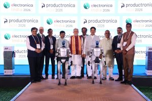
India sharpens its electronics manufacturing edge at electronica India and productronica India 2026 in Greater Noida
- Visitor turnout: 20,922 participants, including key buyers and sourcing decision-makers, turn up for the Greater Noida edition.
- Business engagement: The event facilitated 1,500+ buyer-seller meetings, focused on localisation, supplier discovery, and supply chain partnerships
- International presence: Strong participation from countries like Germany, China, Japan, Taiwan, and the United States
Greater Noida: India’s ambition to position itself as a global electronics manufacturing hub is beginning to reflect in more concrete ways; on factory floors, in policy corridors, and increasingly, on industry platforms where supply chains are being actively reshaped.
The 2026 Greater Noida edition of electronica India and productronica India brought this shift into focus, with a strong turnout of global suppliers, domestic manufacturers, and sourcing leaders. For an industry navigating geopolitical realignments and cost pressures, the event served less as a showcase and more as a working marketplace. The event was attended by 20,922 participants and brought more than 1000+ suppliers and distributors from across the globe and India to the show floor.
The Government of Uttar Pradesh, as the Host State, played a key role in supporting electronica India and Productronica India 2026 in Greater Noida. Its partnership reflected the state’s continued focus on building a strong electronics manufacturing ecosystem, backed by policy support, infrastructure development, and investment facilitation. The presence and involvement of senior government representatives underscored Uttar Pradesh’s intent to position itself as a preferred destination for electronics manufacturing, while also enabling closer engagement between industry stakeholders and policymakers on the ground.
Therefore, the inauguration was led by a cross-section of political and industry leaders, including Shri Suresh Kumar Khanna, Uttar Pradesh’s Minister for Finance and Parliamentary Affairs, and Shri Jitin Prasada, Union Minister of State for Electronics and IT, and for Commerce and Industry. They were joined by Shri Nand Gopal Gupta ‘Nandi’, Minister for Industrial Development; Shri Sunil Kumar Sharma, Minister for IT & Electronics; Shri Ajit Singh Pal, Minister of State for Science and Technology, Electronics and IT; and Shri Alok Kumar, Principal Secretary, IT & Electronics, Uttar Pradesh.
Scale with direction
Across its dual editions in Greater Noida and Bengaluru, the platform now brings together over 60,000 participants annually, reflecting a 50% expansion in scale and reinforcing its position as a key industry meeting point.
The Greater Noida edition saw significant participation from key manufacturing economies, including Germany, China, Japan, Taiwan, and the United States—an indicator of India’s increasing integration into global value chains.
More notably, 1500+ structured and on-ground B2B meetings were conducted during the event, many centred on supplier diversification, localisation strategies, and lead-time optimisation. These are areas that have moved to the top of boardroom agendas as companies reassess dependence on concentrated supply bases.
The current edition reflected a clear emphasis on capability building. Exhibitors pointed to growing interest in component manufacturing, automation, and supply chain resilience. Buyers, particularly from sectors such as automotive and consumer electronics, were seen evaluating domestic suppliers with an eye on long-term partnerships rather than short-term procurement.
Alongside the exhibition, a series of conferences provided a forum for more detailed engagement, aligning with the sector’s current priorities, addressing policy, supply chain resilience, automotive electronics, PCB manufacturing, and advanced production technologies. These themes were explored through platforms such as the UP Electronics Leadership Summit, the ELCINA Supply Chain Summit, the Automotive Display Conference by ICEA, the Bharat PCB Tech Conference, and the SMT Thought Leadership Summit.
The edition also emphasised innovation, featuring a Startup Pavilion supported by the Government of Uttar Pradesh and curated industry podcasts. A notable development was the launch of BPCA, Bharat’s dedicated platform for printed circuits and assemblies, introduced in collaboration with ELCINA and Messe Muenchen India.
Industry bodies such as ELCINA and ICEA were active participants, contributing to both conference discussions and closed-door industry interactions.
Rajoo Goel, Secretary General, ELCINA, stated,“The conversations at electronica India and productronica India 2026 reflected a clear shift in industry priorities. Localisation has moved beyond policy intent and is increasingly becoming a business imperative. The platform brought the value chain together in a way that enabled more practical discussions around strengthening component manufacturing capabilities and reducing external dependencies.”
Pankaj Mohindroo, Chairman, ICEA, added, “What stood out clearly was the growing maturity of India’s electronics ecosystem. We are now seeing a far stronger convergence between policy direction, industry investments, and supply chain strategies, an alignment that is critical for sustainable scale.
electronica and productronica India 2026 played an important role in advancing this momentum by enabling meaningful, direct engagement between global technology and component suppliers and Indian manufacturers who are expanding with long-term commitment and strategic intent.”
Voices from the floor
Participants indicated that the value of the platform lay in the quality of engagement rather than scale alone.
Tsuyuki Junichi – Division Head – Robotics Support Business Division, Yamaha Motor India Sales (P) Ltd said, “For Yamaha Motor India Sales (P) Ltd., electronica India and productronica India, opened more meaningful conversations with teams that are actively planning their next phase of manufacturing growth.”
Mr. Narendra Savant – VP Operations, Kyoritsu Electric India Pvt Ltd stated, “What stood out for us at electronica India and productronica India 2026 in Greater Noida was the clarity of intent from buyers. They came with defined sourcing requirements, timelines, and technical expectations. We saw strong interest across diverse industrial manufacturers for our Customised Robotic + Automation Integrated solutions and our Made-in-India End-of-Line Testers, which aligns with where the Indian electronics manufacturing production needs are heading. For us, the value of this platform lies in the ability to engage with decision-makers who are actively evaluating long-term supply partnerships rather than short-term procurement.”
Raj Kumar Saini – Managing Director, Saini Communications Pvt Ltd, mentioned,“The quality of interaction has definitely gone up. We’re no longer talking about basic automation; most conversations are now around integration, efficiency, and how to scale operations. We’ve had interest coming in from multiple sectors, which is a good sign. You can see that manufacturers are thinking more long-term now, and that changes the kind of discussions you have.”
Visitors highlighted the ability to evaluate global and domestic suppliers within a single platform, enabling faster decision-making.
Robins N T – Head Strategic Sourcing & New Product Development, Simple Energy said, “We are actively looking at diversifying supply chains and increasing localisation, and the interactions here help accelerate that process. The level of preparedness among exhibitors has improved significantly, which makes it easier to move from evaluation to actual business discussions within a short span”.
Srinivasan Sampath – Head NPD Materials at Pricol Limited, said, “What worked well for us at electronica India and productronica India 2026 in Greater Noida was the ability to benchmark multiple suppliers side by side. It helped us compare capabilities, timelines, and approach in a very practical way. In a short span, we were able to narrow down options that would have otherwise taken months to evaluate.”
Anuj Kumar Srivastava – Global Head- Facilities, Secure Meters Ltd. mentioned, “We came in to understand how quickly suppliers in India are adapting to new requirements, especially around quality standards and turnaround times. The interactions here gave us a clearer picture of who is ready to scale and who we can work with as we expand and diversify our operations. Pleased to see focus on Make in India.”
The event also witnessed strategic announcements and MoUs, including expanded collaborations between international PCB and component associations and Indian industry bodies, aimed at strengthening supply chain capabilities and fostering technology exchange.
Dr Reinhard Pfeiffer, CEO, Messe München, said, “What is becoming evident is how quickly India is moving from being part of the conversation about the supply chain to influencing it. Companies no longer assess the country solely based on cost or scale; they are also looking at long-term manufacturing alignment. This shift is reflected in the discussions taking place at electronica India and productronica India 2026 in Greater Noida.”
Bhupinder Singh, President – IMEA, Messe München & CEO, Messe Muenchen India said, “electronica India and productronica India are increasingly reflecting what the industry is dealing with in real time, supply chain adjustments, localisation, and the need for reliable partners. The conversations here are more structured, more practical, and closely linked to actual business decisions, which is where their relevance comes from.”
Looking ahead
The second edition of electronica India and productronica India 2026 is scheduled to be held in Bengaluru from September 16 to 18, 2026, extending the platform’s reach into another major electronics manufacturing hub.
As the industry recalibrates in response to geopolitical and economic shifts, platforms such as these are likely to play a more central role. The question, increasingly, is not whether India will be part of the global electronics supply chain—but how large a role it intends to occupy.
The post India sharpens its electronics manufacturing edge at electronica India and productronica India 2026 in Greater Noida appeared first on ELE Times.
Nuvoton Releases an Industry-Leading-Class High-Power Violet Laser Diode (402 nm, 4.5 W) 1.5 times higher output than our conventional product
Kyoto, Japan, April 15, 2026 – Nuvoton Technology announced today the start of mass production of a “high-power violet laser diode (402 nm, 4.5 W) ” that achieves industry-leading class optical output in a 9.0 mm diameter CAN package (TO-9). This product achieves 1.5 times the optical output compared to our conventional product through our proprietary device structure and heat dissipation design technology, and contributes to improving production throughput in optical equipment such as maskless lithography systems. Furthermore, adding this product to our lineup enables our product portfolio to support major photosensitive materials used in advanced semiconductor packaging.
Achievements:
- Achieves 4.5 W high-power at 402 nm, 1.5 times that of our conventional product, enhancing production throughput in maskless lithography systems
- Expands our lineup of light sources for maskless lithography in advanced semiconductor packaging, supporting multiple major photosensitive materials
- Expands the lineup of mercury lamp replacement solutions [6] , providing new options in light source selection
For more product details, please see here: https://nuvoton.co.jp/semi-spt/apl/rd/?id=1100-0272
Features of New Product:
- Achieves 4.5 W high-power at 402 nm, 1.5 times that of our conventional product, enhancing production throughput in maskless lithography systems
Violet (402 nm) laser diodes generally suffer from relatively low wall-plug efficiency [7] and significant self-heating, and are also prone to short-wavelength-induced degradation, which makes stable high-power operation difficult.
To address these challenges, the “device structure that enhances wall-plug efficiency (WPE)” and the “high thermal conduction package technology that effectively dissipates heat,” which were used in the high-power ultraviolet laser diode [8] (379 nm, 1.0 W) announced as a new product in January 2026, have been expanded to the violet (402 nm) band.
As a result, we are launching a “high-power violet laser diode (402 nm, 4.5 W)” that achieves 1.5 times the optical output compared to our conventional product. In particular, by applying our proprietary facet coating technology that suppresses degradation factors at the laser facets, we have improved the lifetime performance during high-power operation, and by adopting a monolithic molded structure using high heat dissipation materials for the package, we have improved heat dissipation performance.
By achieving both “high-power” and “high reliability”, this product enhances production throughput in industrial optical equipment where high quality is required.
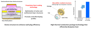
| Figure 1: “Device structure that enhances wall-plug efficiency” and “High thermal conduction package technology that effectively dissipates heat” |
- Expands our lineup of light sources for maskless lithography in advanced semiconductor packaging, supporting multiple major photosensitive materials
This product will deliver significant value in maskless lithography for advanced semiconductor packaging, a market that is rapidly growing, driven by expanding demand for artificial intelligence (AI) and other applications.
In circuit formation for advanced semiconductor packages, maskless lithography technology that directly exposes (draws) wiring patterns based on design data has been attracting attention in recent years, as it enables not only cost reduction and development period shortening, but also high-precision patterning correction in response to substrate warpage and distortion.
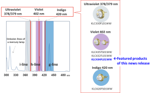
For laser diodes, which are one of the main light sources in this maskless lithography technology, there has been a demand for compatibility with wavelengths close to the i-line (365 nm) and h-line (405 nm), which are the emission lines of mercury lamps, in order to correspond to the main photosensitive materials, as well as higher output for the purpose of improving the production throughput of equipment.
In addition to the “high-power ultraviolet laser diode (379 nm, 1.0 W)” for i-line applications announced in January 2026, we are adding this new product, “high-power violet laser diode (402 nm, 4.5 W) “, for h-line applications to our lineup.
This expansion strengthens our lineup of light sources for maskless lithography in advanced semiconductor packaging, enabling consistent support for multiple major photosensitive materials while contributing to higher production throughput of equipment.
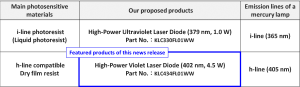
| Table 1: Major Photosensitive Materials in Maskless Lithography for Advanced Semiconductor Packages and Our Proposed Products |
- Expands the lineup of mercury lamp replacement solutions, providing new options in light source selection
This product will be newly added to the lineup of our “semiconductor laser-based alternatives to mercury lamps.” The h-line (405 nm), which is an emission line of mercury lamps, is used in a wide range of fields such as photocuring, 3D printing, sensing, biomedical applications, and marking, and this product provides customers with a new option as an alternative light source for these applications.
Furthermore, by leveraging the high-power performance that is a feature of this product, it will contribute to improving the efficiency of processes that were difficult to realize in the past, as well as to the creation of new optical applications.
| Figure 2: “Mercury Lamp Replacement Solution Using Semiconductor Lasers” Developed by Our Company |
This product is scheduled to be exhibited at our booth at “OPIE’26” to be held in Yokohama, Japan.
Applications:
- Maskless lithography
・ Resin curing
・ Sensing
・ Marking
・ 3D printing
・ Biomedical
・ Alternative light source for mercury lamps, etc.
Product name:
KLC434FL01WW
Specifications:
| Part number | KLC434FL01WW |
| Wavelength | 402 nm |
| Optical Output Power | 4.5 W |
| Package Type | TO-9 CAN |
Start of mass production: May 2026
The post Nuvoton Releases an Industry-Leading-Class High-Power Violet Laser Diode (402 nm, 4.5 W) 1.5 times higher output than our conventional product appeared first on ELE Times.
Mission accomplished: Infineon technology proves reliable once again in space on Artemis II
- Infineon’s radiation-hardened semiconductors performed flawlessly on NASA’s Artemis II Orion capsule across ten days in space.
- Since the 1970s Infineon’s radiation-hardened technology has proven reliable across hundreds of space missions.
- With the world’s first JANS-qualified internally manufactured rad-hard gallium nitride (GaN) transistor, Infineon sets the benchmark for space semiconductors.
Munich, Germany – 15 April 2026 – NASA’s Artemis II mission has successfully returned to Earth after ten days in space, having approached the Moon and reached the farthest distance from our planet ever achieved by crewed spaceflight. The four astronauts have safely returned home, delivering renewed proof that the radiation-hardened (rad-hard) semiconductor solutions of Infineon Technologies AG (FSE: IFX / OTCQX: IFNNY) perform reliably even under the most extreme conditions of deep space. From critical power supply and control systems to data communications, Infineon’s rad-hard devices from its IR HiRel (high reliability) division supported the electronic backbone at the heart of the Orion capsule.
“Space programs require technologies and partners they can rely on for decades. Infineon is a critical technology partner, and we are proud to have once again contributed to the success of a historic space mission,” said Mike Mills, Senior Vice President and General Manager of IR HiRel at Infineon. “The space industry is evolving rapidly: more missions, more data, more electrification – while facing increasing pressure on size, weight and power consumption. In this equation, semiconductors are becoming a central focus in space. The fact that our components performed flawlessly from the first to the last minute of the Artemis II mission is no coincidence. It is the result of decades of engineering expertise, state-of-the-art qualification processes and a deep understanding of what semiconductors must deliver in space.”
Artemis II marks decades of space heritage for Infineon. As far back as the 1970s, Infineon’s predecessor companies supplied the first rad-hard components for NASA and ESA space programs. Since then, Infineon IR HiRel has supported hundreds of space missions including navigation satellites, the International Space Station (ISS), and today’s Artemis program. Our rad-hard components have traveled further than any other human-made object, over 20 billion kilometers from Earth. As a technology leader, Infineon continues to invest in, develop and manufacture the best performing rad-hard semiconductors supporting the space design community on a global scale.
The demands placed on semiconductors in space are immense. Beyond Earth’s protective magnetic field, high-energy particles strike electronic components unimpeded and can permanently damage or destroy them, causing mission failure. Infineon’s rad-hard technology addresses these mechanisms not through passive shielding, but through a semiconductor architecture that is radiation-resistant by design. All products are qualified to the most stringent international space standards, including MIL-PRF-38535 Class V, MIL-PRF-19500, ESA’s ESCC standards and NASA EEE-INST-002, ensuring their reliable performance.
At Infineon, innovation is developed at the system level: semiconductor technology, rad-hard assurance, and packaging perform together. An optimized overall system influences not only electrical performance, but also thermal behavior and long-term reliability – while simultaneously reducing weight and volume. Every gram counts in space, Infineon’s rad-hard parts provide a decisive system-level advantage.
Wide-Bandgap technology: GaN takes the next step
Infineon is also advancing the use of new semiconductor materials in space applications. Gallium nitride (GaN) enables lower switching losses, higher power density and higher switching frequencies – reducing power losses and magnetic component requirements, which translates directly into further weight savings. Built on internal manufacturing capabilities and the process and quality stability that comes with it, Infineon’s award-winning rad-hard 100-V GaN transistor, qualified to JANS (Joint Army Navy Space) per MIL-PRF-19500, brings GaN from concept to proven technology for demanding space missions. Infineon’s JANS qualified device is the first and only internally manufactured rad-hard GaN transistor on the market.
Infineon offers a broad rad-hard portfolio spanning Si power MOSFETs and GaN transistors, gate drivers and solid-state relays, in addition to rad-hard memories and radio frequency (RF) devices. Backed by in-house radiation testing capabilities and guaranteed long-term product availability, Infineon positions itself not merely as a component supplier, but as a strategic technology partner for the entire space industry.
The post Mission accomplished: Infineon technology proves reliable once again in space on Artemis II appeared first on ELE Times.
Bosch and Qualcomm expand collaboration to strategic ADAS solutions
Cockpit Computers: 10 million units delivered
• High-performance solutions: Bosch and Qualcomm aim to make ADAS solutions for enhanced safety and comfort available to everyone
• Continued Business Momentum: Collaboration has secured significant new business wins for both next-generation ADAS and cockpit solutions
• Proven Global Success: Bosch delivers over 10 million cockpit computers powered by Snapdragon Cockpit Platforms
• Global Market Penetration: Deliveries span all vehicle segments from entry to premium, serving both regional and global automakers
Stuttgart, Germany / San Diego, USA – Bosch and Qualcomm Technologies, Inc. announced today that they are expanding their strategic partnership, which has focused on vehicle computers for cockpit solutions, to also include ADAS solutions. Together, Bosch and Qualcomm Technologies are helping address one of the industry’s most pressing needs – scaling intelligent vehicle technology to meet growing consumer demand for vehicles that are automated, connected, and highly personalized. The companies also highlighted a significant milestone in their longstanding collaboration: Bosch has developed and delivered more than 10 million vehicle computers based on Qualcomm Technologies’ Snapdragon Cockpit Platforms for the global automotive market.
“By combining leading-edge compute technology with our system integration expertise – hardware, software, and safety – we enable automakers to meet the rising demand for personalized, safe, and comfortable driving experiences,” said Christoph Hartung, Member of the Bosch Mobility business sector board, Chief Technology Officer for Systems, Software, and Services, and President of the division Cross-Domain Computing Solutions.
“The growing success of our collaboration with Qualcomm Technologies underlines a central value Bosch brings to the industry: we provide the robust, high-performance computing platforms that form the backbone of today’s software-defined vehicle“, said Christoph Hartung, Member of the Bosch Mobility business sector board, Chief Technology Officer for Systems, Software, and Services, and President of the division Cross-Domain Computing Solutions.
“Our collaboration with Bosch spans the full spectrum of vehicle compute – from high‑performance cockpit systems to scalable automated driving solutions and emerging centralized vehicle architectures – all powered by Snapdragon Digital Chassis automotive platforms,” said Nakul Duggal, EVP and Group GM, Automotive, Industrial and Embedded IoT, and Robotics, Qualcomm Technologies, Inc.
“ADAS is where performance and safety must scale in the real world. By expanding our work with Bosch into production-ready ADAS platforms, we’re helping automakers bring advanced driver assistance across vehicle lines more efficiently, with a clear path to centralized compute“, said Nakul Duggal, EVP and Group GM, Automotive, Industrial and Embedded IoT, and Robotics, Qualcomm Technologies, Inc.
Building on this momentum, the companies are extending their collaboration through new ADAS production programs. These programs leverage Bosch’s cost-optimized vehicle computer architecture, powered by Qualcomm Technologies’ Snapdragon Ride platform, to support practical and scalable ADAS deployments. The collaboration also includes purpose-built combined cockpit and ADAS platforms supporting mixed criticality applications delivered on a single system-on-chip, unique to Snapdragon Ride Flex SoCs, aligning with automakers’ software-defined vehicle strategic initiatives. At the core of these programs is the Bosch ADAS integration platform – a scalable, modular vehicle computer designed for ADAS functions. With high bandwidth, computing power, and memory management, it meets strict safety and security standards, fuses multiple sensor technologies for a precise 360° environment model, and runs complex algorithms to deliver safe, dynamic vehicle behavior—even at high speeds.
The Next Frontier: Jointly Engineering the Future of ADAS
Bosch and Qualcomm Technologies’ joint approach is delivering scalable, cost-optimized vehicle computers with ADAS solutions that have secured multiple global customer design wins in the East Asian market. These joint efforts provide automakers with critical flexibility and a clear migration path to centralized computing architectures featuring a small number of highly powerful vehicle computers instead of many individual control units. Powered by the scalable Snapdragon Ride Platform from Qualcomm Technologies, Bosch´s vehicle computers support a broad range of configurations – from entry-level ADAS, such as speed and distance regulation or lane keeping, to advanced automated driving systems. The first vehicles from these new business wins are expected on the road in 2028.
In addition, ADAS and cockpit solutions can also be consolidated onto a single platform to give automakers even greater flexibility and reduce architectural complexity. To this end, Bosch and Qualcomm Technologies are also working on solutions using existing products: Snapdragon Ride Flex builds on this foundation by enabling the consolidation of cockpit and ADAS functions onto a single, safety-certifiable SoC, reducing system complexity, power consumption, and cost while giving automakers a path toward centralized compute architectures. Bosch’s cockpit and ADAS integration platform combines the system functions for assisted and automated driving and infotainment, like personalized navigation and voice assistance functions, in one high-performance computer.
Both the ADAS and cross-domain computing solutions are designed to meet stringent safety requirements (up to ASIL-D) while reducing complexity and cost. For drivers, this means greater access to advanced Level 2 driving features like lane keeping, hands-free driving, and intelligent automated parking.
A story of successful collaboration: defining the modern digital cockpit
The collaboration between Bosch and Qualcomm Technologies is redefining the modern digital cockpit by serving the full spectrum of both the regional and global automotive market across North America, Asia, and Europe. This approach has driven exponential growth since first deliveries began in 2021, scaling from one million units in 2023 to ten million in less than three years, fueled by successful program awards with vehicle manufacturers worldwide. The delivery milestone underscores the companies’ shared ability to industrialize advanced automotive technologies at a global scale for the software-defined vehicle era, spanning entry-level to premium vehicles. The success is rooted in Bosch’s flexible and scalable approach, leveraging Snapdragon Cockpit Platforms. The Bosch cockpit integration platform can drive an increasing number of in-vehicle displays and camera inputs. Qualcomm Technologies’ Snapdragon Cockpit Platforms combine high-performance compute with power-efficient design to enable a wide range of vehicle experiences. That includes crisp, essential displays in cost-optimized systems up to premium systems featuring ultra-low-latency HMI responsiveness, multi-display configurations, immersive multimedia, AI-powered conversational voice assistance, and higher levels of personalization – while maintaining efficiency across vehicle segments.
The post Bosch and Qualcomm expand collaboration to strategic ADAS solutions appeared first on ELE Times.
Gartner Forecasts Worldwide Semiconductor Revenue to Exceed $1.3 Trillion in 2026
- Semiconductor Revenue to Grow 64% in 2026
- DRAM Prices to Increase by 125% in 2026 and Storage Crisis to Extend into 2027
STAMFORD, Conn., April 8, 2026 — Global semiconductor revenue is projected to exceed $1.3 trillion in 2026, exhibiting the highest growth in the last two decades, according to Gartner, Inc., a business and technology insights company.
“Amid high demand for AI processing, data center networking and power, and memory price inflation (memflation), the semiconductor industry is projected to achieve a third consecutive year of double-digit growth in 2026 – a milestone that underscores the sector’s pivotal role in the AI technology stack,” said Rajeev Rajput, Senior Principal Analyst at Gartner.
Gartner forecasts semiconductor revenue will grow 64% in 2026, with memory revenue expected to increase threefold amid memflation (see Table 1). Gartner analysts said that memflation is profound, but it is not perennial. Gartner estimates DRAM and NAND flash annual prices in 2026 will increase by 125% and 234%, respectively, and any meaningful pricing relief is not expected until late 2027.
Table 1. Semiconductor Revenue Forecast, Worldwide, 2025-2027 (Billions in U.S. Dollars)
| 2025 | 2026 | 2027 | |
| Memory | 216.3 | 633.3 | 748.1 |
| Nonmemory | 589.0 | 686.9 | 806.4 |
| Total Market | 805.3 | 1,320.2 | 1,554.5 |
Source: Gartner (April 2026)
AI Semiconductors Will Represent 30% of Total Semiconductor Revenue in 2026
AI semiconductors are expected to account for approximately 30% of total semiconductor revenue in 2026 and will remain the driving force behind the overall industry growth. Hyperscaler investment in AI infrastructure buildouts remains strong, with spending expected to increase by more than 50% in 2026, driving demand for AI accelerators, including GPUs and custom non‑GPU chips.
“Memflation will destroy, or at least delay, non-AI demand into 2028, to varying degrees depending on the application,” said Rajput. “Technology suppliers should prepare for higher prices during the first half of 2026, followed by persistent but moderating price increases throughout the rest of the year. CIOs and IT leaders should be cautious about signing supply agreements with unfavourable pricing terms that extend beyond 2027.”
Gartner clients can read more in Forecast: Semiconductors and Electronics, Worldwide, 2024-2030, 1Q26 and How Long Will AI Demand Sustain Memory Prices.
A complimentary webinar on 1Q26 Semiconductor Reset: Who Wins in a Constrained Market? will take place on April 22 at 11:00 AM ET and registrations are available here.
Gartner Is the World Authority on AI
Gartner is the indispensable partner to C-Level executives and technology providers as they implement AI strategies to achieve their mission-critical priorities. The independence and objectivity of Gartner insights provide clients with the confidence to make informed decisions and unlock the full potential of AI. Clients across the C-Level are using Gartner’s proprietary AskGartner AI tool to determine how to leverage AI in their business. With more than 2,500 business and technology experts, 6,000 written insights, as well as more than 1,000 AI use cases and case studies, Gartner is the world authority on AI. More information can be found here.
The post Gartner Forecasts Worldwide Semiconductor Revenue to Exceed $1.3 Trillion in 2026 appeared first on ELE Times.
STMicroelectronics’ new STM32 series redefines entry-level microcontroller performance and value for smart devices everywhere
- STM32C5 with Cortex®-M33 and 40 nm for enhanced speed and Flash density
- Increased performance with cost efficiency
- Comprehensive ecosystem to enhance end-device capabilities and accelerate time to market
India, April 9, 2026: STMicroelectronics (NYSE: STM), a global semiconductor leader serving customers across the spectrum of electronics applications, has announced a new generation of entry-level microcontrollers (MCUs) to boost the performance of billions of tiny smart devices throughout factories, homes, cities, and infrastructures while meeting extreme cost, size, and power limitations.
The new STM32C5 series is aimed at consumer and professional devices like smart thermostats, electronic door locks, industrial smart sensors, robotic actuators, wearable electronics, and computer peripherals.
“The new STM32C5 elevates the precision, speed, and reliability of competitively priced MCUs to realize the potential in these opportunities. It builds on two decades of STM32 heritage and is part of our ambition to deliver the broadest, most scalable and secure portfolio from entry-level devices to advanced MCUs that redefine the application reach of embedded systems,” said Patrick Aidoune, Group Vice President and General Purpose and Automotive Microcontrollers Division General Manager, STMicroelectronics.
Thanks to an improved design based on ST’s proprietary 40nm manufacturing process, the STM32C5 MCUs can run tasks noticeably faster than many entry-level chips used today. This gives products more room to include modern features such as improved sensing, smoother control, and enhanced user experiences—all while keeping dynamic power consumption low.
The STM32C5 MCUs integrate built-in protections that help safeguard products against tampering and cyber risks. These security features support safer connected devices, a growing priority across consumer and industrial markets.
Users of the new STM32C5 series can enjoy an upgraded STM32Cube environment, now with size-optimized, production-grade drivers to leverage the many hardware features. The modernized ecosystem also introduces enhanced code generation and development tools as well as extended production-ready software examples. Benefiting from continuous updates, the STM32Cube environment is all about helping developers code faster and more efficiently, while maximizing the end-product capabilities.
“At SIT, we work in safety-critical gas and HVAC environments where reliability is essential. For our new generation of Burner Integrated Control platform, choosing the STM32C5 was a natural decision as it provides strong and predictable real-time performance, enabling us to manage combustion, flame detection, and safety interlocks with accuracy, even within a compact footprint. We were able to reuse a large part of our validated firmware, speeding up development, simplifying certification, and the result is a robust and scalable control platform designed for long-term reliability and compliance,” explained Dennis Agnello, Electronics Business Line Director, Heating & Ventilation, SIT Group.
“The STM32C5 provides the performance and feature set enabling us to develop a cost-efficient next-generation AC charger for both public and private use, fully aligned with the latest security, encryption, and interface requirements for metering and EV charging solutions. Throughout the project, ST provided the flexibility and comprehensive ecosystem support we needed to reduce development time and solve key functional and cost challenges to bring our product faster to the market,” said Enrique Osorio, R&D Director, Circontrol (Grupo Circutor).
STM32C5 MCUs are entering production now, targeting packages from 3mm x 3mm UFQFPN20 to 20mm x 20mm LQFP144. STM32 Nucleo evaluation boards, and a display extension board from Riverdi with TouchGFX development software for building entry-level graphical user interfaces, are ready to assist development.
Prices start at $0.64 for orders of 10,000 units.
Technical information
The new STM32C5 MCUs leverage an innovative implementation of the advanced Arm® Cortex®-M33 embedded processor. While ARM’s core delivers advanced performance and efficiency, ST’s proprietary 40 nm manufacturing process is cost-efficient, supports higher clock speeds, and enables memory above 512Kbyte, where lower-density technologies are uncompetitive. STM32C5 MCUs feature on-chip Flash ranging from 128Kbytes, making Cortex-M33 performance accessible at an attractive price for entry-level applications that were previously limited to lower-performing Cortex-M0 and Cortex-M23 devices. Devices are available with up to 1Mbyte, providing generous code and data storage for product designers to create sophisticated new features.
Implementing the Arm Cortex-M33 core at the 40 nm node brings improved arithmetic performance to entry-level devices at a competitive cost and low power. This accelerates computations such as embedded digital filters in sensor signal conditioning, noise suppression, and debouncing. In addition, the power supply scheme, comprising a single low-dropout (LDO) regulator, permits extra user I/O pins. There is also direct memory access (DMA), which helps save power, sharpen system responses, and simplify software. Moreover, with two instances, each having at least four channels to permit two fetches in parallel, DMA on the STM32C5 is a valuable tool for developers to boost application performance.
The MCUs target SESIP3 and PSA Level 3 security certifications, with memory protection, tamper protection, cryptographic engines (symmetrical encryption with AES and hashing algorithm), and temporal isolation (HDP) to protect processes such as secure boot and firmware update. The STM32C59x and STM32C5A3 variants have additional security, including hardware unique key support (HUK), secure key storage, and hardware cryptographic accelerators for symmetric and asymmetric operations with protection against side-channel attacks.
Designed for demanding industrial environments, the device delivers robust performance even in harsh networking conditions. It supports a wide ambient temperature range from -40°C to 125°C, with a junction temperature up to 140°C. Even at the maximum operating temperature, the device can run at its maximum rated frequency, ensuring consistent performance across the full temperature range. STM32C5 enables compliance with industrial safety standards, including IEC 61508 SIL-2 and IEC 60335-1/60730-1 Class-B, by integrating essential hardware and software features.
Enhancements to the development ecosystem include a new STM32CubeMX flavor, STM32CubeMX2, which introduces a preview feature that allows faster access to reference code, thereby accelerating development and easing code reuse. Also new in the STM32CubeC5 embedded software offer, the latest code-size optimized hardware abstraction layer (HAL2) gives access to all MCU features and allows more of the MCU’s memory to be used for application code.
Alex Fabre, Embedded Software Expert at ST Authorized Partner RTONE, has experienced the new tools, commenting: “STM32 HAL2 makes developing with the STM32C5 and other family members faster and more efficient. It is much lighter, closer to hardware functions, and porting our code to other STM32 MCUs is extremely easy.”
The comprehensive ecosystem also gives developers:
- STM32C5 hardware evaluation tools enabling faster prototyping and offering reference hardware design guidelines
• A new examples library offering faster access to a large number of STM32C5 production-ready code examples, simplifying the use of the STM32C5 features and accelerating development
• A choice of two free integrated development environments (STM32CubeIDEand STM32CubeIDE for VSCODE) for faster development and debug
• STM32Cube ecosystem with optimized porting of popular middleware including FreeRTOS, LwIP, USBX, and FileX
About STMicroelectronics
At ST, we are 48,000 creators and makers of semiconductor technologies mastering the semiconductor supply chain with state-of-the-art manufacturing facilities. An integrated device manufacturer, we work with more than 200,000 customers and thousands of partners to design and build products, solutions, and ecosystems that address their challenges and opportunities, and the need to support a more sustainable world. Our technologies enable smarter mobility, more efficient power and energy management, and the wide-scale deployment of cloud-connected autonomous things. We are on track to be carbon neutral in all direct and indirect emissions (scopes 1 and 2), product transportation, business travel, and employee commuting emissions (our scope 3 focus), and to achieve our 100% renewable electricity sourcing goal by the end of 2027. Further information can be found at www.st.com
The post STMicroelectronics’ new STM32 series redefines entry-level microcontroller performance and value for smart devices everywhere appeared first on ELE Times.
Directed Energy Systems: Where Capability Ends and Control Begins
by Sukhendu Deb Roy, Industry Consultant
Key Takeaways- The economics of warfare have flipped, with cost asymmetry emerging as a primary battlefield dynamic
- Directed energy systems shift defence from inventory-driven models to energy-driven ones
- Future defence architectures will be AI-orchestrated, integrated, and multi-domain
- Semiconductor capability is central to defence sovereignty
Modern warfare is undergoing a structural and economic shift—one that is redefining how conflicts are fought and sustained. Across theatres, adversaries are increasingly deploying low-cost, high-volume threats designed not just to penetrate defences, but to exhaust them. This is not merely a tactical evolution; it is an economic strategy aimed directly at the cost structure of defence systems rather than their technical limits.
In response, Directed Energy Weapons (DEW), particularly high-energy laser (HEL) systems, are emerging as a compelling alternative. By reducing the cost per engagement to near-zero and removing dependence on finite ammunition, they signal a transition toward energy-based warfare—where power availability replaces inventory as the primary constraint.
Operational systems today, typically in the 100–300 kW class, are already capable of countering drones, small boats, and select aerial threats. However, their performance remains constrained by power density, beam quality, and thermal dissipation limits.
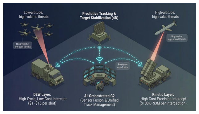
Figure 1. Emerging multi-layered defence architectures integrating kinetic and directed energy systems through AI-driven command and control.
The Problem: Capability Without ControlThis advantage, however, is not absolute. Real-world deployments continue to reveal persistent constraints—thermal limits, atmospheric attenuation, beam dwell time, and power scalability challenges. These are not isolated engineering challenges; they are systemic constraints.
More importantly, they reveal a deeper dependency: the effectiveness of directed energy systems is inseparable from the ecosystem that supports them. Performance is not defined solely by the platform, but by the electronics, semiconductors, and supply chains beneath it.
This creates a structural risk. A nation may deploy advanced directed energy systems, yet remain dependent on external control at the component and semiconductor level.
The future of defence, therefore, will not be determined by the deployment of advanced platforms alone, but by the ability to secure control over the enabling ecosystem that makes those platforms viable at scale.
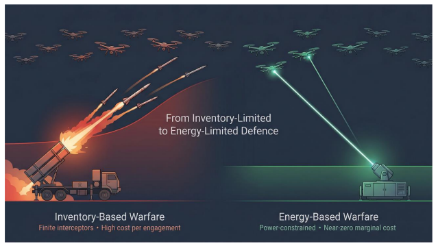
Figure 2. Directed energy systems deliver visible capability, but remain dependent on underlying electronics and semiconductor ecosystems—creating hidden vulnerabilities in control.
The Economic War of AttritionAt the heart of this transformation lies a fundamental imbalance shaping modern conflict. Defenders are increasingly forced to deploy high-value interceptors against low-cost threats, creating an unsustainable economic equation. Systems such as surface-to-air missiles or kinetic interceptors become prohibitively expensive when faced with saturation attacks.
This imbalance is not incidental—it is being deliberately operationalized through drone swarm attacks and loitering munitions designed to overwhelm defences through sheer volume rather than technological sophistication. The objective is clear: to stretch defensive resources to their limits and exploit the cost asymmetry inherent in traditional systems.
Directed energy systems fundamentally alter this equation. By shifting from consumable munitions to energy-based engagement, they dramatically reduce marginal costs and enable sustained operation without the constraints of inventory—as long as sufficient power is available.
This represents more than a technological evolution. It is a financial reset in how defence is structured and sustained. This is the defining shift from inventory-based warfare to energy-based warfare.
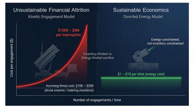
Figure 3. Cost asymmetry in modern warfare—low-cost threats forcing disproportionately expensive kinetic responses, driving unsustainable defence economics.
Without such a transition, the long-term economics of defence operations risk becoming untenable in the face of increasingly scalable, low-cost threats.
The Illusion of SovereigntyThe visible success of a directed energy intercept can be compelling. It signals speed, precision, and technological sophistication—creating the impression of true strategic independence. But that impression can be deceptive.
Beneath every such system lies a tightly integrated ecosystem of power electronics, thermal systems, optical assemblies, RF components, and semiconductors. If these critical elements are externally sourced, control has not been achieved—it has merely shifted out of view. Dependence is not eliminated; it is reconfigured.
In practice, this dependence surfaces through export controls, defence supply chain choke points, firmware constraints, and restricted access to advanced semiconductor nodes. Under normal conditions, these limitations may remain hidden. Under geopolitical stress, they translate directly into operational risk.
Capability alone does not ensure sovereignty.
Control does.
Where Control Actually ResidesTo understand where control truly resides, directed energy systems must be viewed not as standalone platforms, but as layered architectures.
At the surface lies the platform layer—the visible capability, including laser systems deployed on land, sea, or air platforms. Beneath this sits the system layer, where command-and-control frameworks, targeting systems, and sensor fusion enable coordinated operation.
Deeper still is the engineering layer, which determines real-world performance. This includes power electronics that stabilize output, thermal systems that govern endurance, and optical and beam control mechanisms that ensure precision.
At the foundation lies the control layer—the least visible, yet most decisive. This layer encompasses semiconductors, advanced materials, packaging, and the broader supply chain that sustains the system.
It is this lowest layer that anchors performance, scalability, and resilience. Any external dependence here propagates upward, constraining every layer above and limiting true autonomy.
Performance, scalability, and resilience are determined at the lowest layer. Any external dependence at the control layer propagates upward, constraining the entire system.
Sovereignty, in this context, is not a function of the platform—it is a function of control at the component and semiconductor level.
These constraints are not theoretical—they are engineered into the system itself.
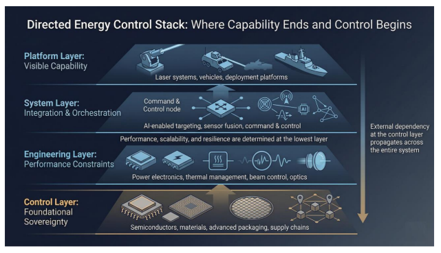
Figure 4. Directed energy performance is constrained by tightly coupled power, thermal, and semiconductor systems—highlighting the central role of control-layer technologies such as GaN-based switching.
The Real BottlenecksThe challenges facing directed energy systems are physical, not conceptual.
- Thermal constraints limit sustained firing duration
- Advanced power electronics define efficiency
- Atmospheric conditions degrade beam propagation
- Beam dwell time limits effectiveness against fast-moving targets
- AI-enabled defence systems must operate at machine speed
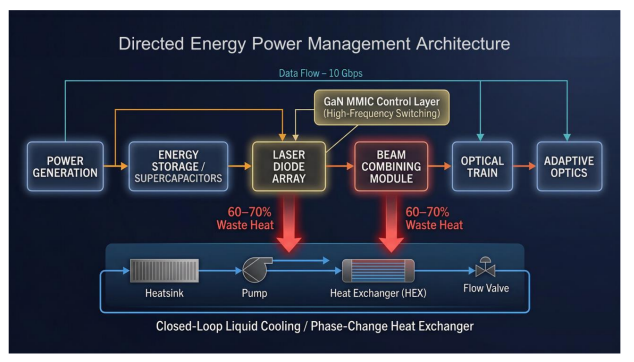
Figure 5. Directed energy constraints are interdependent—thermal, power, and control limitations must be solved as an integrated system, not in isolation.
These constraints do not exist in isolation—they reinforce and amplify one another. Addressing a single limitation, whether in thermal management or power delivery, does not translate into real operational capability on its own. What is required is coordinated industrial depth across multiple domains, from materials science and semiconductor design to power systems and real-time computation.
A directed energy system is only as effective as the ecosystem that sustains it.
From Weapons to SystemsDirected energy is no longer a standalone capability. It is steadily becoming part of integrated, AI-orchestrated defence architectures—often described as Cognitive Hybrid Defence—where multiple systems operate in coordination rather than isolation. In this emerging model, directed energy systems function alongside electronic warfare, cyber capabilities, and kinetic interceptors, all unified through real-time command-and-control frameworks.
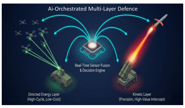
Figure 6. Transition from standalone weapons to AI-orchestrated, multi-layer defence systems, where threats are dynamically assigned to the most efficient response layer.
This shift is already visible in operational programs such as the U.S. Navy’s HELIOS system and Israel’s Iron Beam, both of which demonstrate how layered, multi-domain defence is replacing single-point solutions. The objective is no longer limited to individual interception—it is about orchestrating responses across domains with speed, precision, and economic efficiency. As this transition accelerates, control over the underlying technological ecosystem becomes even more critical.
Semiconductor Policy is Defense PolicyThis convergence carries direct implications for national strategy. Defence capability and semiconductor capability can no longer be treated as separate domains—they are structurally interdependent. Initiatives such as India’s Electronics Component Manufacturing Scheme (ECMS) and the India Semiconductor Mission (ISM 2.0) must be viewed through this lens. These initiatives are central to building semiconductor sovereignty and securing India’s position in the global defence technology supply chain. They are not merely industrial policies; they are foundational to future defence capability.
Yet the challenge is not one of intent or conceptual understanding. It lies in industrial depth—particularly in manufacturing, materials ecosystems, and advanced semiconductor fabrication. Without control over critical technologies such as Gallium Nitride (GaN)-based power electronics systems, advanced packaging, and high-reliability electronics, there is a real risk of remaining a system integrator rather than a true control holder. Sovereignty, in this context, is not achieved through system assembly but through ownership of the components and technologies that define performance and resilience.
Figure 7. Defence capability is fundamentally anchored in semiconductor ecosystems—spanning materials, manufacturing, and advanced power electronics such as GaN-based systems.
Conclusion: Capability vs ControlWhat emerges is a broader shift in how warfare itself is understood. We are moving into a phase defined by energy, integration, and system-level thinking. Directed energy systems will become increasingly visible on the battlefield, delivering immediate and measurable impact. However, the true determinants of success will remain largely invisible—embedded in defence supply chains, semiconductor ecosystems, and industrial capability.
This creates a clear strategic imperative. Nations must move beyond assembling advanced platforms to controlling them end-to-end.
Forward OutlookLooking ahead, the defining question of the next decade will not be who deploys directed energy systems first, but who can sustain and scale them under real-world conditions. Future conflicts may become power-limited rather than ammunition-limited, where grid resilience, energy density, and power electronics infrastructure and power distribution emerge as core defence parameters.
Meeting this challenge will require closer alignment between defence procurement and semiconductor strategy, sustained investment in power electronics, thermal systems, and advanced materials, and a decisive shift from platform-centric thinking to ecosystem-centric design.
Countries that recognize this transition early will build not just capability, but resilience. Those that do not will remain dependent—regardless of how advanced their visible systems may appear.
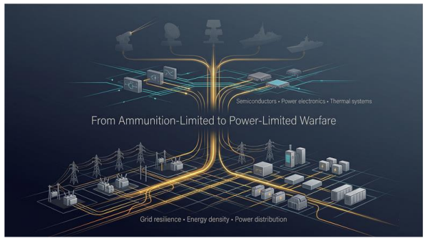
Figure 8. Future defence systems will be constrained by power, energy infrastructure, and semiconductor capability—marking the shift from ammunition-limited to energy-limited warfare.
Final PerspectiveIn the next generation of warfare, capability will be visible. Control will be decisive.
The post Directed Energy Systems: Where Capability Ends and Control Begins appeared first on ELE Times.
Boundary scan in combination with automotive applications for CAN-FD and LIN bus
Serial communication remains the backbone of electronic communication in the automotive sector. The cost-effective LIN bus with master-slave architecture and the fast multi-host fieldbus CAN-FD (Controller Area Network) have become established in this field. The great advantage and efficiency of the applications lies in the combination of both bus systems. GÖPEL electronic has now introduced an extension for the SCANFLEX Multi Port Bus I/O Module 9305 for these interfaces, which makes the functional diversity of the SCANFLEX system available for automotive interfaces in production testing.
With the new BAC module for CAN-FD/LIN, these interfaces can now be tested for functionality during production. The Bus Access Cable (BAC) is connected to one of the five slots of the SCANFLEX Multi Port Bus I/O Module 9305 and thus connected to the SCANFLEX system. This enables access to the complex test functions of the SCANFLEX boundary scan controller. The controller then takes over the simultaneous generation and dynamic distribution of the vectors and control sequences to the interfaces.
SCANFLEX is a modular JTAG/boundary scan controller. Based on state-of-the-art multi-core processors and FPGAs, it allows users to execute test and programming technologies from Embedded JTAG Solutions. Its multifunctional architecture enables these technologies to be combined flexibly and with high performance on a single platform. SCANFLEX II has eight independent, truly parallel test access ports (TAP) for up to 100MHz. This enables the synchronized execution of embedded test, debug, and programming operations via boundary scan (IEEE1149.x), processor emulation, chip integrated instruments, or the embedded diagnostics method.
About GÖPEL electronic
GÖPEL electronic develops and manufactures innovative electrical and optical test, measurement, and inspection equipment for electronic components and printed circuit board assemblies as well as industrial and automotive electronics systems. The company is active worldwide, with its own subsidiaries as well as through distributors, and generated sales of approximately 40 million euros in 2023 with 240 employees.
The post Boundary scan in combination with automotive applications for CAN-FD and LIN bus appeared first on ELE Times.
Why Every EV & 5G Phone Could Soon Be Powered by Gujarat
In a move that cements India’s transition from a consumer to a producer in the global silicon race, Prime Minister Narendra Modi officially inaugurated the Kaynes Semicon OSAT (Outsourced Semiconductor Assembly and Test) facility on March 31, 2026.
The ₹3,300 crore plant, located in the industrial heart of Sanand, marks the second major semiconductor unit to go operational in Gujarat within 900 days, following the earlier launch of the Micron facility. This rapid execution underscores the momentum of the India Semiconductor Mission (ISM) 2.0, as the country aggressively pursues a slice of the $110 billion global chip market.
A Global Export HubWhile domestic self-reliance is a key driver, the Kaynes plant is looking outward. During the ceremony, the first batch of Intelligent Power Modules (IPMs), sophisticated components that integrate 17 individual chips, was presented to Stephen Chang, CEO of Alpha & Omega Semiconductor, a California-based anchor customer.
“Today, a new bridge has been formed between Sanand and Silicon Valley,” the Prime Minister stated during his address. “The modules made here will reach American companies and, from there, power the world.”
Key Specifications of the Sanand PlantThe facility is designed for high-volume, high-precision manufacturing, focusing on sectors that are currently seeing explosive growth:
| Feature | Details |
| Investment | ₹3,300 Crore |
| Production Capacity | Approx. 6.3 Million chips per day |
| Primary Products | Intelligent Power Modules (IPMs), Multi-chip modules |
| Target Industries | Electric Vehicles (EVs), Industrial Automation, 5G Infrastructure |
| Timeline | From Cabinet approval to production in 14 months |
The inauguration is more than just a corporate milestone; it is a strategic piece of the “India Techade” vision. Unlike traditional manufacturing, the Kaynes plant focuses on the back-end of the semiconductor value chain, like assembly, testing, and packaging, which has historically been a bottleneck for Indian electronics.
Union IT Minister Ashwini Vaishnaw highlighted the speed of the project, noting that the plant moved from foundation-laying to commercial production in record time. He also pointed to the growing “Sanand-Dholera” cluster, which is being modelled after global hubs like Hsinchu in Taiwan and Gyeonggi in South Korea.
Building the Talent PipelineTo sustain this growth, Kaynes Semicon announced a memorandum of understanding with SVNIT Surat to develop a specialised workforce. This partnership aims to bridge the gap between academic theory and the rigorous standards of semiconductor cleanrooms, ensuring a steady stream of engineers for the 10 major chip projects currently approved across six Indian states.
As the ribbon was cut in Sanand, the message to the global tech community was clear: India is no longer just waiting for the future of hardware; it is assembling it.
The facility has already reported early execution success, having shipped approximately 900 multi-chip modules (IPM5) just days before the formal inauguration, signalling high operational readiness for its export commitments.
By: Shreya Bansal, Sub-Editor
The post Why Every EV & 5G Phone Could Soon Be Powered by Gujarat appeared first on ELE Times.
WSCAD ELECTRIX AI Cuts 50% Engineering Effort For Alligator Automations
Alligator Automations India Pvt. Ltd., a manufacturer of end-of-line packaging automation systems, has reduced engineering effort in electrical design by around 50% by implementing WSCAD’s E-CAD solution.
The company’s ten-person electrical engineering team now uses WSCAD for creating electrical schematics, control cabinet design, and project documentation. Previously, tasks such as wire numbering, device grouping, and bill-of-materials generation had to be performed manually, resulting in project delays and an increased risk of errors. After switching to WSCAD, many of these steps are now automated, significantly improving both efficiency and design accuracy.
“Tasks that previously required manual work are now automated,” says Sagar Bhavsar, Control Engineering Manager at Alligator Automations. “Wire numbering alone now takes roughly half the time, allowing our team to focus more on complex design and optimisation tasks.”
Alligator Automations develops customised automation solutions, including robotic palletising systems, packaging automation, automatic loading systems, and intralogistics conveyor technology. Projects cover the entire value chain – from design and development to manufacturing, installation, commissioning, and long-term support for customers in industries such as food & beverage, paint & cement, fertiliser & petrochemicals, as well as tyre and agro industries.
“Automation projects are becoming increasingly complex while engineering timelines continue to shrink,” says Dr Axel Zein, CEO of WSCAD. “At the same time, AI is fundamentally changing how electrical engineering is performed. By automating documentation, verification, and knowledge retrieval, engineers can focus more on system design and optimisation instead of repetitive tasks. The Alligator Automations example demonstrates how standardising the E-CAD environment can significantly increase engineering efficiency.”
Beyond schematic creation, WSCAD supports precise 2D and 3D control cabinet layouts, automatic wire routing, and direct data transfer to cabinet manufacturing systems. This eliminates media discontinuities and reduces sources of error. AI-supported design, documentation, and multilingual translation capabilities further accelerate project delivery while ensuring compliance and data quality.
The post WSCAD ELECTRIX AI Cuts 50% Engineering Effort For Alligator Automations appeared first on ELE Times.
Vishay Intertechnology Automotive Grade Photovoltaic MOSFET Driver Boosts Reliability and Lowers Costs in High Voltage Systems
Vishay Intertechnology has introduced a new Automotive Grade photovoltaic MOSFET driver that is the first such device in the compact SMD-4 package to provide a creepage distance of 8 mm and mould compound with a comparative tracking index (CTI) of 600. Designed to increase safety and reliability in high voltage automotive applications — while simplifying designs and reducing costs — the Vishay Semiconductors VODA1275 features the industry’s fastest turn-on times and the highest open circuit voltage and short circuit current in its class.
Classified as providing reinforced isolation, the device delivers an open circuit voltage of 20 V typical, short circuit current of 20 μA, and turn-on time of 80 μs, which is three times faster than competing devices. These characteristics enable quicker and more reliable driving of MOSFETs and IGBTs in high-voltage systems. In addition, the device’s working isolation voltage of 1260 Vpeak and isolation test voltage of 5300 VRMS make it ideal for 800 V+ battery systems.
AEC-Q102 qualified, the VODA1275 is intended for use in pre-charge circuits, wall chargers, and battery management systems (BMS) for electric (EV) and hybrid electric (HEV) vehicles. While designers previously had to use two MOSFET drivers in series to generate the higher voltages required in these applications, the device’s high open-circuit output voltage allows them to use just one, saving space and lowering costs. In addition, the driver enables the creation of custom solid-state relays to replace legacy electromechanical relays in next-generation vehicles.
The optically isolated VODA1275 draws all the current required to drive its internal circuitry from an infrared emitter on the low-voltage side of the isolation barrier. This construction simplifies designs and lowers costs by eliminating the need for an external power supply. The MOSFET driver is RoHS-compliant, halogen-free, and Vishay Green.
The post Vishay Intertechnology Automotive Grade Photovoltaic MOSFET Driver Boosts Reliability and Lowers Costs in High Voltage Systems appeared first on ELE Times.
ROHM has added New Lineup of 17 High-Performance Op Amps Enhancing Design Flexibility
ROHM has added the new CMOS Operational Amplifier (op amp) series “TLRx728” and “BD728x” to its lineup. These are suitable for a wide range of applications, including automotive, industrial, and consumer systems. A broad lineup also makes product selection easier.
In recent years, demand for high-accuracy op amps has been rapidly increasing as automotive and industrial systems become more sophisticated, demanding faster speed, better precision, and higher efficiency. In applications requiring amplification of sensor outputs, minimising signal error and delay is essential. To meet these requirements, a well-balanced set of key characteristics is needed, including Input Offset Voltage, Noise, and Slew Rate.
These new products are high-performance op amps that offer a low input offset voltage, low noise, and high slew rate. TLRx728 features an input offset voltage of 150 μV (typ.), while the BD728x offers 1.6 mV (typ.). Both series have a noise voltage density of 12 nV/√Hz at 1kHz and a slew rate of 10 V/μs. They are therefore suitable for a wide range of precision applications, including sensor signal processing, current detection circuits, motor driver control, and power supply monitoring systems. Both series are designed to balance versatility and high performance rather than being limited to specific applications.
Application Examples
Automotive equipment, industrial equipment, and consumer electronics.
Example use case: Sensor signal processing, current detection circuits, motor driver control, and power supply monitoring systems.
The post ROHM has added New Lineup of 17 High-Performance Op Amps Enhancing Design Flexibility appeared first on ELE Times.
Govt Infuses ₹258 Crore Into 128 Startups to Drive DeepTech and IP Creation
In a major move to solidify India’s standing as a global high-tech hardware hub, the Union Government has announced a strategic investment of ₹257.77 crore (approximately $31 million) into 128 technology startups.
The announcement, shared by Minister of State for Electronics and IT, Jitin Prasada, in a written reply to the Rajya Sabha on Friday, March 27, 2026, highlights a shift toward “risk capital” for sectors critical to national security and economic self-reliance.
The “Fund of Funds” MechanismThe investment was executed through the Electronics Development Fund (EDF), which operates under a “Fund of Funds” model. Instead of direct equity, the EDF acts as an anchor investor in eight professionally managed “Daughter Funds” (early-stage venture and angel funds).
These Daughter Funds have leveraged the government’s initial contribution to mobilise a total of ₹1,335.77 crore in follow-on investments for startups specialising in:
-
Semiconductor Design & Nano-electronics
-
Cybersecurity & AI/ML
-
Robotics & IoT
-
Medical Electronics (HealthTech)
As of late February 2026, the ripple effect of this capital injection has already yielded significant socio-economic returns:
-
Job Creation: Over 22,700 high-skilled jobs have been generated within the supported startups.
-
Intellectual Property: The companies have successfully filed or acquired more than 300 IPs, reinforcing India’s domestic design capabilities.
-
Profitable Exits: The government has already realised ₹173.88 crore from 37 successful exits, proving that DeepTech ventures are becoming increasingly viable for investors.
While the government aims for pan-India growth, the current investment data shows a strong concentration in existing tech corridors. Bangalore remains the undisputed leader, housing 88 of the 128 funded startups.
A Strategic Pivot Toward Self-RelianceThis news comes on the heels of the Ministry of Electronics and IT (MeitY) approving 29 additional projects under the Electronics Component Manufacturing Scheme, involving a cumulative investment of ₹7,104 crore.
By focusing on the “Daughter Fund” model, the government ensures that capital is managed by industry experts while maintaining a minority stake—a move designed to encourage private venture capital to take more “brave” bets on hardware and indigenous R&D rather than just consumer-facing software apps.
“The goal is to build a self-sustaining electronics ecosystem,” stated the Ministry. “We aren’t just looking for the next ‘unicorn’; we are looking for the next breakthrough in Indian-owned IP.”
By: Shreya Bansal, Sub-Editor
The post Govt Infuses ₹258 Crore Into 128 Startups to Drive DeepTech and IP Creation appeared first on ELE Times.
Nuvoton Launches Upgraded Driving Smart Device, NuMicro M3331 Series MCU
As the global transition toward industrial automation and smart living accelerates, the security and processing efficiency of microcontrollers (MCUs) have become decisive factors for enterprises’ success in the business-to-business market. Nuvoton Technology has announced the launch of its new NuMicro M3331 series 32-bit microcontroller. Powered by the Arm Cortex-M33 core, the M3331 series delivers exceptional performance at operating frequencies of up to 180 MHz and integrates TrustZone technology, providing a robust hardware foundation for industrial control, smart factories, smart buildings, and renewable energy.
The M3331 series is more than just a hardware platform; it is an integrated solution designed to address the challenges customers face when processing complex control algorithms and protecting intellectual property (IP). Featuring the Cortex-M33 core with built-in DSP instruction set and a single-precision floating point unit (FPU), it runs up to 180 MHz. The M3331 series is built with comprehensive security mechanisms. Through hardware-level Secure Boot, it ensures that the system executes only certified and authorised firmware from startup, establishing an immutable root of trust. To protect core IP assets, it features eXecute-Only-Memory (XOM) to safeguard core algorithms and eliminate the risk of code leakage. Additionally, the TrustZone technology partitions a secure execution environment to effectively defend against malicious attacks.
Designed for reliability, the M3331 series supports a wide operating temperature range from -40°C to +105°C and exhibits superior interference resistance (ESD HBM 4 kV / EFT 4.4 kV), significantly reducing the risk of downtime caused by environmental factors. To further enhance system reliability, the 512 KB Flash memory supports Error Correction Code (ECC) for detecting and repairing bit-flip errors. Furthermore, within the 320 KB SRAM, a hardware parity check is provided for the 64 KB core area, achieving true industrial-grade system resilience.
To meet the diverse communication demands of the IoT era, the M3331 series introduces an I3C interface and two CAN FD controllers, greatly increasing data throughput between sensors and control nodes. For high-speed peripherals and mass storage, it includes a built-in USB 2.0 High-Speed OTG controller (with on-chip PHY) and an SDH (Secure Digital Host Controller) interface, delivering exceptional performance for both gaming products requiring low-latency transmission and smart consumer devices needing high-bandwidth storage.
Moreover, the M3331 series features a 12-bit ADC with a sampling rate of up to 4.2 Msps, accurately capturing subtle changes in analogue signals. With up to 48 PWM outputs, it provides precise control solutions for professional photography lighting and stage lighting. Specifically, the series is equipped with ELLSI (Enhanced LED Light Strip Interface) and up to 10 LLSI (LED Light Strip Interface) interfaces, supporting next-generation gaming ARGB LED control protocols. This offloads the CPU and reduces development difficulty, enabling brilliant and fluid dynamic LED effects. The M3331 series offers a variety of package options, from the compact QFN 33 (4×4 mm) to the high-pin-count LQFP 128 (14×14 mm), helping customers optimise their PCB layouts.
To accelerate time-to-market, Nuvoton provides NuMaker-M3333KI and NuMaker-M3334KI evaluation boards, along with full support for mainstream RTOS (FreeRTOS, Zephyr, RT-Thread) and GUI libraries (emWin, LVGL). This ecosystem empowers customers to build stable system solutions rapidly.
The M3331 series consists of two subseries: the M3333 series (without USB 2.0 support) and the M3334 series (with USB 2.0 support).
The post Nuvoton Launches Upgraded Driving Smart Device, NuMicro M3331 Series MCU appeared first on ELE Times.
India Boosts Tech Manufacturing: Government Approves 29 New Electronics Component Projects Worth ₹7,100 Crore
In a significant move to fortify India’s position as a global electronics hub, the Ministry of Electronics and IT (Meity) has approved 29 new applications under its flagship component manufacturing scheme.
The announcement, made on Monday by IT Secretary S. Krishnan, marks a substantial expansion of the nation’s industrial capacity. The newly sanctioned projects represent a cumulative investment of ₹7,104 crore, signalling robust private sector confidence in the government’s “Make in India” initiatives.
Economic Impact and Job CreationThe scale of the approved projects is expected to ripple through the domestic economy. According to Secretary Krishnan, the fresh wave of investment is projected to:
-
Generate 14,246 new jobs directly within the electronics manufacturing segment.
-
Yield a production value of ₹84,515 crore, significantly reducing reliance on imported sub-assemblies and parts.
This latest round of approvals brings the total number of sanctioned projects under the Meity scheme to 75. By focusing specifically on components—the building blocks of smartphones, computers, and automotive electronics—the government aims to move beyond simple assembly and build a more resilient, end-to-end domestic ecosystem.
“The approval of these 29 applications underscores our commitment to deepening the electronics value chain in India,” a senior official noted, highlighting that the move is a strategic step toward the country’s goal of reaching a $300 billion electronics production target by 2026.
The scheme continues to be a cornerstone of India’s strategy to compete with regional manufacturing giants, providing the necessary fiscal support to offset the high costs of setting up sophisticated component units.
The post India Boosts Tech Manufacturing: Government Approves 29 New Electronics Component Projects Worth ₹7,100 Crore appeared first on ELE Times.
STMicroelectronics expands 800 VDC AI datacenter power conversion portfolio with new 12V and 6V architectures in collaboration with NVIDIA
STMicroelectronics has announced the expansion of its 800 VDC power conversion portfolio with two new advanced architectures: 800 VDC to 12V and 800 VDC to 6V. Developed according to the NVIDIA 800 VDC reference design, these new power conversion stages complement the previously introduced 800 VDC to 50V solution. The rapidly emerging 800 VDC data centre architecture enables higher energy efficiency, reduces power losses, and supports more scalable, high compute density infrastructure for hyperscalers and AI compute.
“As AI infrastructure compute scale continues to expand fast, it requires higher voltage distribution and greater density, which can only be achieved with system-level innovation for each of the different AI server form factors,” said Marco Cassis, President, Analog, Power & Discrete, MEMS and Sensors Group Head of STMicroelectronics’ Strategy, System Research and Applications, Innovation Office at STMicroelectronics. “With these new converters for 800 VDC power distribution, ST brings a complete set of solutions to support the deployment of gigawatt-scale compute infrastructure with more efficient, scalable, and sustainable power architectures.”
A complete 800 VDC ecosystem for the different AI server form factors
The expansion to 12V and 6V output stages reflects the industry move toward different server architectures requiring different power delivery topologies depending on GPU generation, server height, form factor, and thermal envelope for large-scale training clusters, inference farms, and high-density AI infrastructures. The 50V, 12V, and 6V intermediate DC buses will all coexist in AI data centres depending on rack density, GPU configuration, and cooling strategy.
The new 800 VDC to 12V converter enables high-efficiency distribution from rack-level power shelves directly to the voltage domains that feed advanced AI accelerators.
The new 800 VDC to 6V path allows OEMs to reduce the number of conversion stages and move the 6V bus closer to the GPU. This reduces copper usage, minimises resistive losses, and improves transient performance, a critical differentiator for large-scale training clusters.
Back in October 2025, STMicroelectronics introduced a fully integrated prototype power‑delivery system showcasing a compact GaN‑based LLC converter operating directly from 800 V at 1 MHz with over 98% efficiency and exceptional power density in a smartphone‑sized footprint exceeding 2,600 W/in³ at 50 V.
The three solutions combine ST technologies across power semiconductors (silicon, SiC, GaN), analogue and mixed-signal, and microcontrollers.
Technical highlights of the new 12V and 6V architectures
Direct 800 VDC to 12V high-efficiency conversion:
- Eliminates the traditional 54V intermediate stage, reducing conversion steps and system-level losses.
- Enables higher rack-level efficiency, lower copper usage, and simplified integration for future GPU generations.
- Includes a newly developed high-density power delivery board (PDB) achieving efficiency targets exceeding the sum of the previous two-stage conversion paths.
800 VDC to 6V architecture for GPU-nearing conversion:
- Is designed for system builders who require power stages closer to the GPU, minimising IR drop and improving response under fast load transients.
- Completes the topology portfolio for servers with ultra-dense GPU configurations.
The post STMicroelectronics expands 800 VDC AI datacenter power conversion portfolio with new 12V and 6V architectures in collaboration with NVIDIA appeared first on ELE Times.
Сторінки

