
ELE Times

One Nation, One Compute Grid: India’s Leap into the AI and Supercomputing Era
Courtesy: Dr. Harilal Bhaskar, Chief Operating Officer (COO) and National Coordinator at I-STEM (Indian Science Technology and Engineering facilities Map) under the Office of Principal Scientific Adviser (P.S.A.) Government of India.
When Talent Meets Infrastructure
In a small university town in Bihar, a student dreams of designing renewable energy systems. She excels at theory and design, yet her laptop freezes during large-scale MATLAB simulations. In Andhra Pradesh, a doctoral scholar struggles to check her thesis against plagiarism databases because her institution lacks adequate licenses.
Meanwhile, across the world, peers in the United States, Europe, and China train artificial intelligence models on GPU clusters, run exascale climate simulations, and test quantum algorithms. The difference is not in talent—it is in infrastructure.
Innovation today is constrained not by ideas but by access to computing power. India’s researchers, start-ups, and students face uneven access to high-performance computing (HPC), AI platforms, and quantum resources. This gap threatens to widen inequality and slow national progress.
The Vision: A National Digital Commons
India’s answer is a federated national compute grid—a seamless network connecting supercomputers, AI labs, and emerging quantum facilities. Instead of duplicating procurement, ultra-expensive research platforms such as ANSYS Enterprise Suite, Dassault BIOVIA/SIMULIA, Schrödinger Drug Discovery, or quantum-grade simulation packages like VASP could be shared through centralized national licenses, reducing million-dollar expenditures while ensuring equitable access for researchers across domains.
Imagine the possibilities:
- A climate scientist in Assam running continental-scale simulations on a Bengaluru supercomputer.
- A linguist in Nagaland applying AI-powered text analytics without local infrastructure.
- A start-up in Pune experimenting with quantum testbeds via a national portal.
Such an ecosystem transforms access from privilege to commons, ensuring geography or budget does not decide opportunity.
Why Now: The Strategic Imperative
The global race for computational power is accelerating:
- United States: The NSF and Department of Energy provide access to some of the world’s fastest AI and supercomputing resources.
- European Union: The EuroHPC initiative builds exascale-ready systems while fostering cross-border collaboration.
- China: National HPC and quantum centres are aligned with industrial strategy and defence priorities.
India cannot afford fragmented approaches. A One Nation–One Compute Grid would unify HPC clusters, AI labs, quantum resources, and software licenses into a scalable, efficient national framework.
Current status underscores urgency: India’s most powerful system, PARAM Siddhi-AI, ranks only around 60th globally, far behind US and Chinese peers. Under the National Supercomputing Mission, 18 HPC systems have been deployed, but gaps remain in accessibility, GPUs, and quantum nodes. Without scale and coordination, India risks lagging behind in AI-driven innovation.
A National HPC–AI–Quantum Portal
Modern research in genomics, climate science, or AI requires resources far beyond individual labs. A National Compute Portal could:
- Catalogue available compute clusters, GPUs, and quantum nodes.
- Provide automated scheduling for resource booking.
- Allow priority allocation for urgent national missions (pandemic modelling, energy transition).
- Embed AI-guided support for booking and troubleshooting.
- Supply policymakers with dashboards for monitoring usage, efficiency, and outcomes.
This portal would serve as the command centre of India’s scientific computing ecosystem.
Building Skills and Human Capital
Infrastructure without skilled manpower risks underutilization. Alongside the portal, India must:
- Expand HPC/AI training programs in IITs, NITs, and universities.
- Develop quantum algorithm bootcamps for researchers and start-ups.
- Create national fellowships for AI-HPC specialists to ensure talent pipelines.
This ensures that the grid is not just available, but also actively and effectively used.
AI Labs, Industry Integration, and Regional Balance
HPC thrives when connected to broader ecosystems:
- Start-ups can test AI or quantum algorithms without heavy capital costs.
- Universities and national labs can pool datasets and compute power.
- Sector-specific labs—in health, climate, finance, cybersecurity—can run experiments at scale with real-world impact.
Equity must be central:
- Tier-2 and Tier-3 cities should gain equal access through the portal.
- Incentives must support rural and state universities, ensuring inclusion beyond elite IIT/IISc clusters.
Here, HPC and AI infrastructure are the engines, while software serves as a supporting layer.
Governance, Security, and Funding Models
A unified system requires layered governance:
- Central Government: anchor investments, negotiate national licenses, and set mission priorities.
- Institutions: contribute idle compute cycles and avoid duplication.
- Industry and CSR programmes: co-invest in AI accelerators, GPUs, and quantum nodes.
- Oversight: embed cybersecurity, fair-use policies, and ethical AI standards.
Security and sovereignty must be priorities:
- Strong encryption and access controls.
- Safeguards for genomic, financial, and citizen datasets.
- Alignment with India’s Digital Personal Data Protection Act (DPDPA, 2023).
Funding pathways could include:
- Public–private partnerships for data centres.
- Corporate CSR support for compute nodes.
- A “compute credit” model, where researchers and start-ups receive national cloud-like credits.
Learning from Global Models
- United States: Federated HPC networks maximize scale and reach.
- European Union: Cross-border HPC integration builds resilience and efficiency.
- China: Strategic placement of HPC and quantum centres accelerates industrial outcomes.
India can draw from all three—combining scale, inclusivity, and strategic alignment—into one unified ecosystem.
Sustainability and Green Computing
HPC centres are energy-intensive. To align with India’s climate commitments, the grid should:
- Use renewable-powered data centres.
- Incentivize energy-efficient GPUs and low-carbon quantum hardware.
- Deploy AI to optimize energy scheduling and cooling.
This ensures that innovation does not come at the cost of sustainability.
Global Collaboration
A national compute grid strengthens India’s role in global alliances:
- Participation in BRICS quantum/HPC research.
- Collaborations with the QUAD on AI standards.
- Bilateral HPC/quantum projects with partners like Japan, US, and EU.
India’s unified grid would make it a preferred partner in global science and innovation diplomacy.
The Payoff: Democratization and Innovation
A One Nation–One Compute Grid would:
- Democratize access to HPC, AI, and quantum platforms.
- Accelerate patents, research output, and industrial prototypes.
- Strengthen academic integrity with AI-powered plagiarism detection.
- Optimize the National Supercomputing Mission and quantum initiatives.
- Cut redundant spending on licenses and infrastructure.
- Empower start-ups, SMEs, and industry to innovate at scale.
- Ensure balanced regional development and global competitiveness.
The outcome is a knowledge republic, where innovation flows from ideas—not from institutional budgets or geography.
Conclusion: Building the Knowledge Republic
India has already transformed governance and finance with Aadhaar and UPI. The next frontier is research infrastructure.
A One Nation–One Compute Grid—anchored in HPC, AI labs, and quantum computing, and strengthened by shared software, skilled manpower, and green sustainability—can redefine India’s place in global innovation.
The real question is not whether India can build this system.
The question is: Can India afford not to?
The post One Nation, One Compute Grid: India’s Leap into the AI and Supercomputing Era appeared first on ELE Times.
CEA-Leti & STMicroelectronics’ Demonstrate Path to Fully Monolithic Silicon RF Front-Ends with 3D Sequential Integration at IEDM 2025
CEA-Leti and STMicroelectronics showcased key enablers for a new high-performance and versatile RF Si platform cointegrating best-in-class active and passive devices used in RF and Optical FEM at IEDM 2025. Their paper detailed 3D sequential integration of silicon-germanium (SiGe) heterojunction bipolar transistors (HBT), RF SOI switches, and high-quality passives on a single wafer—opening a path to highly integrated, low parasitic, and targeting cost-efficient systems for next-generation wireless and wireline communications.
The paper, “Unlocking High-Performance Si RF Platforms with SiGe HBT and RFSOI Switch Technologies,” described the methodology to directly build high-performance components on the same silicon wafer rather than packaged or stacked as separate chips. This can be achieved through 3D sequential integration, which layers different device types, such as SiGe HBT and SOI CMOS switches, without overheating the lower tiers during processing.
‘Efficient and Cost-Effective’
“Our team has shown that high-performance SiGe HBT has been conceived to be compatible with the top-tier fabrication steps, and that trap-rich isolation can be localized and thermally robust, and low-temperature (600°C) SOI switches can match state-of-the-art figures of merits,” said CEA-Leti’s Thibaud Fache, lead author of the paper. “These results pave the way to an all-silicon RF front-end module that is efficient and cost-effective.”
The team showed that a localized trap rich layer can achieve RF isolation and linearity comparable to costly commercial trap-rich substrates, while withstanding thermal cycles up to 600 °C—preserving the performance of the underlying SiGe HBT layer.
‘From Advanced Research to Manufacturable Solutions’
By extending silicon’s reach of sequential integration into the RF domain, the CEA-Leti/ST team’s work points to a future of more accessible, energy-efficient connectivity. Fully integrated RF and optical front ends could simplify the manufacturing and enable cost-effective deployment of dense wireless networks essential for smart cities, autonomous systems, and AI datacenters.
“This joint result demonstrates a credible path from advanced research to manufacturable solutions,” said ST’s Thomas Bordignon, co-author of the paper. “By combining CEA-Leti’s sequential integration know-how with ST’s RF technology expertise, we’re enabling the co-integration of state-of-the-art SiGe HBT, switches and passive devices, that are key elements of the FEM.”
Materials Science Milestone
Achieving a performant RF Partially Depleted (PD) SOI switch at 600 °C rather than standard ~1000 °C is a first. It is worth noting that process flow of this low-temperature device does not rely on new equipment or costly steps and is thus quickly industrially viable thanks to the relatively relaxed thermal budget constraints of bottom tier (600°C). The team demonstrated high-quality, low-loss RF switches fabricated at 600 °C, maintaining the performance of the SiGe HBT below and confirming the feasibility of a fully integrated silicon RF platform.
Additional Breakthrough Presentation
CEA-Leti researchers will report tomorrow a major breakthrough (session 33-4) with the design of high-performance silicon-on-insulator (SOI) MOSFETs processed at 400°C. NMOS and pMOS transistors demonstrate state-of-the art performances among the Back-End-Of-Line devices, fulfilling all industrial figures of merit without any compromise. This reliable versatile analog transistor targets More Than Moore applications bringing differential advantage for smart sensors, near memory computing and RF devices.
The post CEA-Leti & STMicroelectronics’ Demonstrate Path to Fully Monolithic Silicon RF Front-Ends with 3D Sequential Integration at IEDM 2025 appeared first on ELE Times.
New, Imaginative AI-enabled satellite applications through Spacechips
As the demand for smaller satellites with sophisticated computational capabilities and reliable along with robust onboard processor systems to support the five to ten-year duration of a mission grows, so does the limits of the latest ultra‑deep‑submicron FPGAs and ASICs and their power delivery networks. These high-performance processors have demanding, low-voltage, high-current power requirements and their system design is further compounded by the complexities of managing thermal and radiation conditions in space.
To cater to these demands, Spacechips has introduced its AI1 transponder, a small, on-board processor card containing an ACAP (Adaptive Compute Acceleration Platform) AI accelerator. The smart, re-configurable receiver and transmitter delivers up to 133 tera operations per second (TOPS) of performance that enables new Earth-observation, in-space servicing, assembly and manufacturing (ISAM), signals intelligence (SIGINT), and intelligence, surveillance and reconnaissance (ISR) and telecommunication applications to support real-time, autonomous computing while ensuring the reliability and longevity to complete longer missions.
“Many spacecraft operators simply don’t have sufficient bandwidth in the RF spectrum to download all of the data they’ve acquired for real-time processing,” said Dr. Rajan Bedi, CEO of Spacechips. “An alternative solution is accomplishing the processing in-orbit and simply downlink the intelligent insights.”
New levels of processing power spawn imaginative new applications in space and on Earth
Today’s low-Earth-orbit observation spacecraft can establish direct line of sight over a specific region only about once every ten minutes. If satellites were trained to fill those blind spots using AI algorithms, emergency management teams could make faster, better-informed decisions when direct line-of-sight communication with Earth is not possible. Spacechips is harnessing these powerful artificial intelligence compute engines to enable in-orbit AI to address a variety of Earth-bound and space-related problems:
- Tracking space debris to avoid costly collisions
- Monitoring mission critical spacecraft system health
- Identifying severe weather patterns
- Reporting critical crop production rainfall data
 Figure 1 On-orbit AI can detect temperature anomalies such as wildfires, volcanic activity, or industrial accidents with the Spacechips AI1 processer. This helps emergency management teams make faster, better-informed decisions about which fire prone areas are the most vulnerable.
Vicor Factorized Power Architecture delivers high current, low voltage
Given the constrained operating environment of space, AI-enabled computing has an acute need for precision power management. The need is compounded by the expanding number, scope and variety of missions that require different kinds of spacecraft and a growing reliance on some form of solar power to deliver adequate power.
This led Spacechips to partner with Vicor to incorporate Vicor Factorized Power Architecture (FPA) using high density power modules into the Spacechips AI1 Transponder Board. FPA is a power delivery system design that separates the functions of DC-DC conversion into independent modules. In Vicor’s radiation tolerant modules, the bus converter module (BCM) provides the isolation and step down to 28V, while the pre-regulator module (PRM) provides regulation to a voltage transformation module (VTM) or current multiplier that performs the 28V DC transformation to 0.8V.
The value of the Vicor solution, according to Bedi, is that it is very small and power dense. This allows for better efficiency and flexibility by reducing size and weight and yields higher power density, especially in high-performance computing applications.
By adopting Vicor’s FPA power delivery system, Bedi is helping telecommunications and SIGINT operators perform real-time, on-board processing by autonomously changing RF frequency plans, channelization, modulation and communication standards based on live traffic needs. Vicor power converter modules also feature a dual powertrain, which for fault-intolerant space applications provides built-in redundancy that allows loads to be driven at 100 percent on each side of the powertrain.
 Figure 2 Vicor Factorized Power Architecture (FPA) separates the functions of DC-DC conversion into independent modules. Using radiation-tolerant modules, the BCM bus converter provides the isolation, the PRM regulator provides the regulation and the VTM current multiplier performs the DC transformation. This allows for better efficiency, flexibility and higher power density, especially in high-performance computing applications.
“Vicor FPA delivers a much more elegant, efficient solution in a very small form factor,” Bedi said. “The benefits of Vicor FPA are simply an order of magnitude superior to everything else on the market.”
Together Spacechips and Vicor have partnered to design the most power-dense, reliable processer board on orbit. The AI1 board is rad-tolerant, rugged and compact. It sets a new standard for power processing, enabling the next-generation of computing and application design for New Space.
The post New, Imaginative AI-enabled satellite applications through Spacechips appeared first on ELE Times.
Fighting Fire with Fire: How AI is Tackling Its Own Energy Consumption Challenge to Boost Supply Chain Resilience
AI is no longer just a futuristic idea, today it is a known technology across every industry. AI is being used to automate tasks, make quicker decisions, and build digital products that were once considered impossible to create. But as AI becomes more common, a major problem is starting to show up: it uses a lot of energy. Training large models and keeping them running day and night requires huge amounts of computing power, which in turn puts pressure on power grids, data centres, and the supply chains that support them.
This creates a clear paradox. AI demands significant energy, yet it can also help organisations manage energy more efficiently. With data centre power requirements expected to rise sharply, procurement teams, engineers, and supply chain leaders must reconsider how AI systems are designed, deployed, and supported. Encouragingly, low-power AI architectures and smarter data-centre management tools are emerging to tackle the issue from within the ecosystem.
Energy Consumption Profile of AI Technologies
AI’s energy demand has surged as newer models grow larger and more compute-intensive. Boston Consulting Group reports that U.S. data centers consumed about 2.5% of national electricity in 2022, a share projected to rise to nearly 7.5% around 390 TWh by 2030.
The biggest contributors include:
- Model Training
Training today’s large models isn’t a simple overnight job. It involves running thousands of GPUs or specialised AI chips in parallel for weeks at a stretch. The compute load is enormous, and the cooling systems have to run constantly just to stop the hardware from overheating. Together, they draw a surprising amount of power.
- Data Center Operations
People often assume most of the power goes into the servers, but the cooling and air-handling equipment consume almost as much. As AI traffic grows, data centers are forced to maintain tight temperature and latency requirements, which makes the power bill climb even faster.
- Inference at Scale
Running models in real time, or inference, now accounts for most of AI’s total energy consumption. With generative AI being used in search engines, content creation tools, manufacturing systems, and supply chain operations, continuous inference tasks place constant pressure on electricity infrastructure.
AI-Driven Strategies for Energy EfficiencyTo mitigate AI’s energy consumption, several AI-driven strategies have been developed:
- Energy-Efficient Model Architectures
Modern AI research increasingly focuses on architectures that deliver higher performance with lower computational load. Techniques gaining wide adoption include:
- Pruning: Removing redundant neurons and parameters to shrink model size.
- Quantization: Reducing precision (e.g., FP32 → INT8) with minimal accuracy loss.
- Knowledge Distillation: Compressing large teacher models into compact student models.
These approaches can cut training and inference energy by 30–60%, making them critical for enterprise-scale deployments.
- Adaptive Training Methods
Adaptive training methods dynamically adjust GPU allocation, batch size, and learning rate based on convergence behavior. Instead of running training jobs at maximum power regardless of need, compute intensity scales intelligently. This prevents over-provisioning, lowers operational costs, and reduces carbon footprint particularly in cloud-based AI development workflows.
- AI-Powered Data Center Energy Management
AI is increasingly being integrated into Hyperscale data-centre control systems because it can monitor operations faster than humans. It tracks power usage, detects irregularities, and predicts demand spikes so workloads and cooling can be adjusted before issues arise.
Google applied this approach in its facilities and found that machine-learning–based cooling adjustments reduced energy use by about 15–20%. According to Urs Hölzle, this improvement came from predicting load changes and tuning cooling in advance.
- Cooling System Optimization
Cooling is one of the largest energy loads in data centres. AI-driven cooling systems, especially those using offline reinforcement learning, have achieved 14–21% energy savings while maintaining thermal stability.
Techniques include:
- Predicting thermal hotspots
- Dynamic airflow and coolant modulation
- Intelligent chiller sequencing
- Liquid-cooled rack optimization
As AI model density increases, these innovations are essential for maintaining operational uptime.
- Predictive Analytics for Lead Time Optimization
AI forecasting tools optimize procurement, lead time, and logistics by predicting:
- Seasonal energy price fluctuations
- Grid availability
- Renewable energy generation patterns
- Peak demand windows
These insights allow organizations to schedule compute-heavy workloads like model training-during low-cost or low-emission energy periods, directly improving supply chain resilience
Strategic Implications for Procurement and Supply Chain ManagementEnergy-efficient AI is not merely an IT requirement; it is a supply chain strategy. Organizations are rethinking how they source hardware, design workflows, and plan operations.
1. Procurement of Energy-Efficient Semiconductors
The demand for low-power AI accelerators and CPUs-such as Arm Neoverse platforms is rising sharply. Procurement leaders must prioritize vendors who offer:
- High performance-per-watt
- Advanced power management features
- Hardware-level AI acceleration
Selecting the right semiconductor partners reduces long-term operational costs and aligns with sustainability commitments
- Enhancing Supply Chain Resilience
Energy availability and cost volatility can trigger delays, downtime, and disruptions. AI-based energy optimization enhances resilience by:
- Predicting shortages
- Reducing load on critical systems
- Identifying alternative low-power workflows
- Optimizing backup generation or renewable energy use
This is particularly vital for semiconductor fabs, logistics hubs, and manufacturing plants that rely on uninterrupted power.
- Wafer Fab Scheduling Analogies
The semiconductor industry offers a useful analogy: wafer fabrication requires meticulous scheduling to optimize throughput while managing energy-intensive processes. AI-driven energy management requires:
- Workload balancing
- Thermal and power constraint management
- Predictive scheduling
- Minimization of idle compute cycles
Several trends are shaping the next wave of AI energy innovation:
1. Specialized Low-Power AI Chips
Arm, NVIDIA, AMD, and start-ups are designing AI chips focused on maximum efficiency per watt-critical for both data centers and edge AI systems.
2. Green Data Centers
Operators are investing in:
- Renewable power
- Liquid immersion cooling
- Waste heat reuse
- Modular micro-data centers
These reduce operational emissions and increase grid independence.
3. Regulatory Pressures
Governments are introducing stricter carbon reporting, energy consumption caps, and sustainability requirements—pushing organizations toward greener AI adoption.
4. Market Volatility
Energy price fluctuations directly impact the cost of training and deploying AI. Organizations must adopt agile, energy-aware planning to maintain competitiveness.
ConclusionAI is in a strange position right now. On one hand, it consumes a huge amount of energy; on the other, it’s one of the best tools we have for cutting energy waste. When companies use more efficient model designs, smarter data-center management systems, and predictive tools that anticipate resource needs, they can bring down operating costs and make their supply chains more stable.
Using sustainable AI isn’t just a “good to have” anymore it’s becoming a key factor in staying competitive. As businesses push deeper into digital operations, the combination of AI innovation and energy-conscious thinking will play a major role in determining which organisations stay resilient and which ones fall behind.
The post Fighting Fire with Fire: How AI is Tackling Its Own Energy Consumption Challenge to Boost Supply Chain Resilience appeared first on ELE Times.
Beyond the Bill: How AI-Enabled Smart Meters Are Driving Lead Time Optimization and Supply Chain Resilience in the Energy Grid
Introduction
Smart meters have significantly evolved since their initial implementation for consumer billing. In the contemporary networked industrial landscape, where semiconductor fabrication facilities, data centers, and manufacturing plants rely on a consistent, high-quality electrical supply, AI-enabled smart meters have become essential instruments. These meters, integrated with edge analytics, IoT infrastructures, and cloud-based machine learning engines, produce high-resolution data that informs procurement, operational planning, and supply chain resilience.
For the semiconductor industry, where a single hour of downtime in a wafer fab can cost between $1–5 million, energy reliability is not merely operational, it is existential. By using predictive analytics from AI-enabled smart meters, both utilities and semiconductor fabs gain visibility into consumption anomalies, voltage instability, and equipment stress patterns that traditionally led to delays, yield losses, and unplanned shutdowns.
As Dr. Aaron Shields, Director of Grid Strategy at VoltEdge, remarks-For semiconductor fabs, energy intelligence is no different from process intelligence. AI-enabled metering is now a supply chain stabilizer, not just a measurement tool.
Smart Meters as Intelligent, High-Resolution Energy Nodes
Smart Meters as Sophisticated, High-Resolution Energy Nodes
Contemporary AI-driven smart meters possess integrated processors, edge AI chips, and secure communication protocols. These qualities convert them into “micro-decision engines” capable of executing:
- Local anomaly detection
- High-frequency load forecasting
- Voltage quality assessment
- DER coordination
- Event-driven grid signalling
This is especially important for semiconductor ecosystems, which need very careful monitoring because they are very sensitive to voltage drops, harmonics, and micro-interruptions.
Semiconductor fabs typically run:
- 5,000–50,000 process tools,
- under strict schedule windows,
- where wafer fab scheduling depends on consistent energy flow to keep lithography, etching, CMP, and deposition tools stable.
AI-enabled smart meters supply real-time, tool-level and grid-level data that feeds these scheduling algorithms, reducing cycle time disruptions.
AI Applications for Grid Optimization and Semiconductor Supply Chain Stability
Through a number of methods, AI-enabled smart meters improve supply chain resilience in the utility and semiconductor manufacturing industries.
Predictive Maintenance & Equipment Lead Time Planning
AI detects early signatures of:
- transformer fatigue,
- feeder overloads,
- harmonic distortions,
- and breaker stress.
Utilities can then predict how many spare parts they will need and speed up the delivery of important parts. Semiconductor fabs likewise gain advance warning for facility equipment—HVAC loads, chillers, pumps, and vacuum systems.
Demand Forecasting with Industry-Specific Models
AI models like LSTM, transformer networks, and hybrid ARIMA-ML pipelines look at things like:
- Patterns in the production cycle
- Peak fab energy windows
- Changes in seasonal demand
- Large tool starts up currents
- Changes in the grid at the level of the grid
Better energy forecasting helps fab procurement leaders get power contracts, make better energy-based costing models, and cut down on delays caused by volatility.
Risk Mitigation During Market Volatility
Changes in energy prices have a direct effect on the costs of making chips. AI-AI-driven intelligent metering offers:
- Early warnings of grid instability
- Risk maps highlighting feeders that could trigger fab downtime
- Real-time dashboards for emergency preparedness
This improves the stability of the semiconductor supply chain amid energy price volatility or grid congestion events..
Case Study 1: European Utility + Semiconductor Fab Partnership Reduces Lead Times by 28%
A prominent European utility implemented AI-integrated smart meters throughout the industrial area containing a semiconductor fabrication facility with a capacity of 300,000 wafers per month. Historically, unpredictable transformer failures forced the fab to activate emergency procurement workflows.
AI-driven meter analytics identified transformer strain 18 days prior to conventional SCADA systems
This gave the utility’s purchasing team the ability to:
- Reorder transformer modules ahead of time
- Reduce urgent shipment costs
- Avoid fab shutdowns
Result:
- 28% reduction in transformer component lead times
- Zero unplanned fab downtime in eight months
- 12% improvement in wafer fab scheduling adherence
Case Study 2: Indian Fab Achieves 22% Faster Spare-Part Fulfilment Using Smart Meter Predictive Analytics
AI-enabled smart meters were installed from substation to tool-level feeders at a semiconductor fab park in India. Unusual starting-current spikes in the CMP and deposition sections were detected by predictive analytics, suggesting impending breaker degradation.
The fabs supply chain leaders integrated this data into their ERP procurement engine.
Impact:
- Spare-part availability increased by 24%
- Maintenance response times improved by 22%
- Downtime during voltage sag occurrences lowered by 17%%
The park’s engineering head noted: “Intelligence from smart meters now directs our procurement schedule.” We strategize weeks in advance, rather than hours.
Strategic Insights for Procurement Leaders Across Energy & Semiconductor Sectors
- Granular consumption data facilitates precise procurement. Prediction Meter data facilitates the prediction of:
Meter data helps forecast:
- Spare-transformer needs
- HVAC load cycles
- Cleanroom energy peaks
- Fuel windows for backup generators
This facilitates long-term vendor agreements and minimizes unanticipated orders.
- Smarter Vendor Evaluation
Tool uptime and voltage stability data allow semiconductor fabs to evaluate how supplier components behave under real load conditions.
- Lead Time Optimization Through Predictive Insights
Early detection of energy-side failures prevents:
- Wafer batches that are late,
- Cycle times that are too long, and
- Tool requalification delays.
Utility supply chains also reduce buffer stocks while improving availability.
- Operational Resilience and Risk Mitigation
AI-enabled data supports:
- Contingency planning
- Load re-routing
- Rapid DER activation
- Process tool safeguarding
This is crucial in a sector where milliseconds of voltage fluctuation can scrap millions in wafers.
Future Trends: Where Energy Intelligence Meets Semiconductor Precision
- AI-Orchestrated Load Scheduling for Fabs
Predictive models will align fab tool scheduling with energy stability windows. - Digital Twins Using Smart Meter Data
Utilities and fabs will run simulations to test equipment stress scenarios before making procurement decisions. - Edge AI Advancements
Next-generation meters will host larger models that independently diagnose harmonic distortions critical to lithography and etching tools. - Real-Time ROI Dashboards
CFOs in the semiconductor sector will see energy risk reduction as a way to get a good return on investment.
Conclusion
Artificial intelligence-enabled smart meters are essential for the modernization of the electricity grid and the stabilization of the semiconductor supply chain. Procurement directors, supply chain strategists, and fabrication engineers can make informed, proactive decisions with access to real-time analytics, predictive maintenance metrics, and load forecasting information. Smart meters are increasingly essential for maintaining production schedules, reducing lead times, and remaining competitive globally, as wafer manufacture requires consistent, high-quality power.
The post Beyond the Bill: How AI-Enabled Smart Meters Are Driving Lead Time Optimization and Supply Chain Resilience in the Energy Grid appeared first on ELE Times.
Inside the Digital Twin: How AI is Building Virtual Fabs to Prevent Trillion-Dollar Mistakes
Introduction
Semiconductor manufacturing often feels like modern alchemy: billions of tiny transistors squeezed onto a chip smaller than a fingernail, stitched through thousands of precise steps. Shifting a line by nanometres can ruin the batch.
The stakes are enormous. One day of unplanned downtime in a top fab can wipe out over $20 million. Problems aren’t always dramatic shutdowns; sometimes, process drift quietly eats into yields, totalling billions in lost revenue yearly. Factor in easily wobbling supply chains, and you see the industry’s looming “trillion-dollar risk.”
AI-powered digital twins are living mirrors of the factory. Continuously updated with real data, they run endless “what-if” scenarios, catching errors before they become costly. It’s like rehearsing production virtually, avoiding real-world mistakes.
- What is a Digital Twin in Semiconductor Manufacturing?
Now, a digital twin in a fab isn’t just some fancy simulation it’s basically a virtual twin of the whole facility, kept in lockstep with the real thing. Traditional simulations? They’re kind of frozen in time. Digital twins, on the other hand, are always moving, always learning, pulling in data from thousands of sensors, tool logs, and manufacturing systems to really reflect what’s happening on the floor.
Their scope is huge. For instance:
- Wafer Fab Scheduling: Figuring out the best sequence and queue times across hundreds of tools, shaving days off wafer cycles that can otherwise drag past 90 days.
- Tool Behavior Simulation: Watching how lithography, etching, and deposition tools drift or wear out, and guessing when they’ll need attention.
- Predictive Maintenance: Catching potential failures before they hit, avoiding downtime that could grind production to a halt.
The cool part? They keep getting smarter. Every wafer that runs through the fab teaches the twin a little more, helping it predict better and suggest fixes before things go sideways. Over time, fabs move from constantly reacting to actually staying ahead of the game.
- How AI Makes Digital Twins Smarter
AI is the real power that changes things. Digital twins transition from mere reflections to autonomous control systems capable of independent decision-making.
For instance:
- Defect Prediction: Machine learning spots tiny defect patterns humans or simple rules miss. A lithography misalignment, for instance, is caught before it ruins wafers.
- Automated Calibration: Reinforcement learning algorithms fine-tune deposition or etch times, keeping precision high with minimal human input.
- Fab Simulation: You can stress-test entire fabs virtually (temperature, vibration, purity changes) to see how production fares.
The impact is real:
- 30% faster validation, qualifying new processes quicker.
- 25% better yield forecasts, cutting waste.
- Avoided downtime over $2 million per tool daily (SEMI data).
AI tools like Bayesian models and reinforcement learning push fabs toward self-regulation—the factory learns to heal itself. The workflow below shows how AI twins turn raw data into better supply chain outcomes.

Figure 1: AI-powered digital twins connect fab data, predictive analytics, and real-time simulation to deliver measurable gains in yield, procurement efficiency, and supply chain resilience.
- Procurement & Supply Chain Resilience
The engineering benefits of digital twins are clear, but they also bring unexpected value to procurement and supply chain planning, functions exposed as fragile during the pandemic-era chip shortage.
- Supplier Qualification: Before approving new photoresists, gases, or wafers, digital twins simulate their impact on yield, reducing the risk of supplier-induced disruptions.
- Equipment Sourcing: AI predicts the saturation point of tools, enabling fabs to place orders in advance and avoid expensive overstocking.
- Virtual Commissioning: Tools can be simulated in the digital twin prior to acquisition, guaranteeing return on investment and compatibility with current production lines.
Case Study: When advanced lithography tools ran short in 2021, a major foundry used its twin to re-sequence wafer queues. This move held throughput steady, saved nearly $5 million in delay costs, and kept chips on schedule.
The globalization of supply chains necessitates this foresight. A firm in Taiwan can now anticipate the effects of a European chemical delay weeks in advance and adjust wafer production schedules to mitigate losses.
- Future Outlook: Virtual Fabs, Resilience, and ESG
The goal is the “virtual-first fab.” Every new process or recipe must be fully tested in the twin before going live. That method sharply lowers risk and cuts the cost of old-school trial-and-error.
Beyond efficiency, twins are crucial for sustainability targets:
- Scrap: Less wafer loss helps factories cut material scrap by 5–10%.
- Energy: Better tuning and scheduling can drop energy use by 3–7% per wafer.
- Waste: Fewer reworks directly cuts chemical and water usage.
Rahimian and other experts say that smart fabs of the future will combine efficiency with resilience, making supply chains stronger and better for the environment.
- Challenges on the Road Ahead
Despite their promise, setting up and maintaining a digital twin system is tough.
- Data Silos: Merging data from specialized, unlike tools is the core issue. Many factories use older equipment that lacks common data formats.
- Computational Demands: Running high-fidelity twins needs exascale computing, which smaller operations can’t afford.
- Adoption Hurdles: The industry needs simple rules for interoperability. Plus, veteran engineers must trust AI over their experience.
Solving this requires equipment makers, software firms, and chip producers to collaborate. Groups like SEMI are already pushing for common standards.
- Visualizing the Future
To see the full potential, think of a digital dashboard for a modern fab operator:
A heatmap shows when the wafer queue will be full, so there is no chaos. 3D models forecast tool wear weeks in advance. A supply chain radar tracks every bottleneck like a neon shortage or logistics delay in real time.
These visuals change factories from reactive spaces to proactive ecosystems. Every worker can now anticipate and adapt to changes, instead of constantly fighting crises.
Conclusion
The semiconductor industry drives nearly every modern device, yet its manufacturing risks are enormous. Digital twins are becoming essential because they let engineers spot yield problems early, see where supply issues may emerge, and keep sustainability efforts on track. These models aren’t just virtual copies of factories; they give teams clearer insight into how to run tools, materials, and workflows more efficiently and with fewer surprises. As digital-twin technology matures, it’s set to influence how leading fabs plan, test, and refine production. The message is clear: manufacturing’s future isn’t only physical. It’s virtual-first, AI-validated, and designed to prevent trillion-dollar mistakes.
The post Inside the Digital Twin: How AI is Building Virtual Fabs to Prevent Trillion-Dollar Mistakes appeared first on ELE Times.
Open World Foundation Models Generate Synthetic Worlds for Physical AI Development
Courtesy: Nvidia
Physical AI Models- which power robots, autonomous vehicles, and other intelligent machines — must be safe, generalized for dynamic scenarios, and capable of perceiving, reasoning and operating in real time. Unlike large language models that can be trained on massive datasets from the internet, physical AI models must learn from data grounded in the real world.
However, collecting sufficient data that covers this wide variety of scenarios in the real world is incredibly difficult and, in some cases, dangerous. Physically based synthetic data generation offers a key way to address this gap.
NVIDIA recently released updates to NVIDIA Cosmos open-world foundation models (WFMs) to accelerate data generation for testing and validating physical AI models. Using NVIDIA Omniverse libraries and Cosmos, developers can generate physically based synthetic data at incredible scale.
Cosmos Predict 2.5 now unifies three separate models — Text2World, Image2World, and Video2World — into a single lightweight architecture that generates consistent, controllable multicamera video worlds from a single image, video, or prompt.
Cosmos Transfer 2.5 enables high-fidelity, spatially controlled world-to-world style transfer to amplify data variation. Developers can add new weather, lighting and terrain conditions to their simulated environments across multiple cameras. Cosmos Transfer 2.5 is 3.5x smaller than its predecessor, delivering faster performance with improved prompt alignment and physics accuracy.
These WFMs can be integrated into synthetic data pipelines running in the NVIDIA Isaac Sim open-source robotics simulation framework, built on the NVIDIA Omniverse platform, to generate photorealistic videos that reduce the simulation-to-real gap. Developers can reference a four-part pipeline for synthetic data generation:
- NVIDIA Omniverse NuRec neural reconstruction libraries for reconstructing a digital twin of a real-world environment in OpenUSD, starting with just a smartphone.
- SimReady assets to populate a digital twin with physically accurate 3D models.
- The MobilityGen workflow in Isaac Sim to generate synthetic data.
- NVIDIA Cosmos for augmenting generated data.
From Simulation to the Real World
Leading robotics and AI companies are already using these technologies to accelerate physical AI development.
Skild AI, which builds general-purpose robot brains, is using Cosmos Transfer to augment existing data with new variations for testing and validating robotics policies trained in NVIDIA Isaac Lab.
Skild AI uses Isaac Lab to create scalable simulation environments where its robots can train across embodiments and applications. By combining Isaac Lab robotics simulation capabilities with Cosmos’ synthetic data generation, Skild AI can train robot brains across diverse conditions without the time and cost constraints of real-world data collection.
Serve Robotics uses synthetic data generated from thousands of simulated scenarios in NVIDIA Isaac Sim. The synthetic data is then used in conjunction with real data to train physical AI models. The company has built one of the largest autonomous robot fleets operating in public spaces and has completed over 100,000 last-mile meal deliveries across urban areas. Serve’s robots collect 1 million miles of data monthly, including nearly 170 billion image-lidar samples, which are used in simulation to further improve robot models.
See How Developers Are Using Synthetic Data
Lightwheel, a simulation-first robotics solution provider, is helping companies bridge the simulation-to-real gap with SimReady assets and large-scale synthetic datasets. With high-quality synthetic data and simulation environments built on OpenUSD, Lightwheel’s approach helps ensure robots trained in simulation perform effectively in real-world scenarios, from factory floors to homes.
Data scientist and Omniverse community member Santiago Villa is using synthetic data with Omniverse libraries and Blender software to improve mining operations by identifying large boulders that halt operations.
Undetected boulders entering crushers can cause delays of seven minutes or more per incident, costing mines up to $650,000 annually in lost production. Using Omniverse to generate thousands of automatically annotated synthetic images across varied lighting and weather conditions dramatically reduces training costs while enabling mining companies to improve boulder detection systems and avoid equipment downtime.
FS Studio partnered with a global logistics leader to improve AI-driven package detection by creating thousands of photorealistic package variations in different lighting conditions using Omniverse libraries like Replicator. The synthetic dataset dramatically improved object detection accuracy and reduced false positives, delivering measurable gains in throughput speed and system performance across the customer’s logistics network.

Robots for Humanity built a full simulation environment in Isaac Sim for an oil and gas client using Omniverse libraries to generate synthetic data, including depth, segmentation and RGB images, while collecting joint and motion data from the Unitree G1 robot through teleoperation.

Omniverse Ambassador Scott Dempsey is developing a synthetic data generation synthesizer that builds various cables from real-world manufacturer specifications, using Isaac Sim to generate synthetic data augmented with Cosmos Transfer to create photorealistic training datasets for applications that detect and handle cables.

Conclusion
As physical AI systems continue to move from controlled labs into the complexity of the real world, the need for vast, diverse, and accurate training data has never been greater. Physically based synthetic worlds—driven by open-world foundation models and high-fidelity simulation platforms like Omniverse—offer a powerful solution to this challenge. They allow developers to safely explore edge cases, scale data generation to unprecedented levels, and accelerate the validation of robots and autonomous machines destined for dynamic, unpredictable environments.
The examples from industry leaders show that this shift is already well underway. Synthetic data is strengthening robotics policies, improving perception systems, and drastically reducing the gap between simulation and real-world performance. As tools like Cosmos, Isaac Sim, and OpenUSD-driven pipelines mature, the creation of rich virtual worlds will become as essential to physical AI development as datasets and GPUs have been for digital AI.
In many ways, we are witnessing the emergence of a new engineering paradigm—one where intelligent machines learn first in virtual environments grounded in real physics, and only then step confidently into the physical world. The Omniverse is not just a place to simulate; it is becoming the training ground for the next generation of autonomous systems.
The post Open World Foundation Models Generate Synthetic Worlds for Physical AI Development appeared first on ELE Times.
How Well Will the Automotive Industry Adopt the Use of AI for its Manufacturing Process
Gartner believes that by 2029, only 5% of automakers will maintain strong AI investment growth, a decline from over 95% today.
“The automotive sector is currently experiencing a period of AI euphoria, where many companies want to achieve disruptive value even before building strong AI foundations,” said Pedro Pacheco, VP Analyst at Gartner. “This euphoria will eventually turn into disappointment as these organizations are not able to achieve the ambitious goals they set for AI.”
Gartner predicts that only a handful of automotive companies will maintain ambitious AI initiatives after the next five years. Organizations with strong software foundations, tech-savvy leadership, and a consistent very long-term focus on AI will pull ahead from the rest, creating a competitive AI divide.
“Software and data are the cornerstones of AI,” said Pacheco. “Companies with advanced maturity in these areas have a natural head start. In addition, automotive companies led by execs with strong tech know-how are more likely to make AI their top priority instead of sticking to the traditional priorities of an automotive company.”
Fully-Automated Vehicle Assembly Predicted by 2030
The automotive industry is also heading for radical operational efficiency. As automakers rapidly integrate advanced robotics into their assembly lines, Gartner predicts that by 2030, at least one automaker will achieve fully automated vehicle assembly, marking a historic shift in the automotive sector.
“The race toward full automation is accelerating, with nearly half of the world’s top automakers (12 out of 25) already piloting advanced robotics in their factories,” said Marco Sandrone, VP Analyst at Gartner. “Automated vehicle assembly helps automakers reduce labor costs, improve quality, and shorten production cycle times. For consumers, this means better vehicles at potentially lower prices.”
While it may reduce the direct need for human labor in vehicle assembly, new roles in AI oversight, robotics maintenance and software development could offset losses if reskilling programs are prioritized.
The post How Well Will the Automotive Industry Adopt the Use of AI for its Manufacturing Process appeared first on ELE Times.
Electronics manufacturing and exports grow manifold in the last 11 years
Central government-led schemes, including PLI for large-scale electronics manufacturing (LSEM) and PLI for IT hardware, have boosted both manufacturing and exports in the broader electronics category and the mobile phone segment.
The mobile manufacturing in India has taken a tremendous rise. In last 11 years, total number of mobile manufacturing units have increased from 2 to more than 300. Since the launch of PLI for LSEM, Mobile manufacturing has increased from 2.2 Lakh Cr in 2020-21 to 5.5 Lakh Cr.
Minister of State for Electronics and Information Technology Jitin Prasada, in a question, informed Rajya Sabha on Friday that as a result of policy efforts, electronics manufacturing has grown almost six times in the last 11 years – from ₹1.9 lakh crore in 2014-15 to ₹11.32 lakh crore in 2024-25.
The booming industry has generated employment for approximately 25 lakh people and the electronic exports have grown by eight times since 2014-15.
According to the information submitted by Union Minister for Electronics and Information Technology Shri Ashwini Vaishnaw in Rajya Sabha, to encourage India’s young engineers, the Government is providing latest design tools to 394 universities and start-ups. Using these tools, chip designers from more than 46 universities have designed and fabricated the chips using these tools at Semiconductor Labs, Mohali.
Also, all major semiconductor design companies have set up design centers in India. Most advanced chips such as 2 nm chips are now being designed in India by Indian designers.
The post Electronics manufacturing and exports grow manifold in the last 11 years appeared first on ELE Times.
Taiwanese company to invest 1,000 crore in Karnataka for new electronics & semiconductor park
Allegiance Group signed a Memorandum of Understanding (MoU) with Karnataka to develop an India-Taiwan Industrial Park, creating a dedicated hub for advanced electronics and semiconductor manufacturing.
Karnataka has secured a major foreign investment with Taiwan-based Allegiance Group signing an MoU to establish a ₹1,000-crore India-Taiwan Industrial Park (ITIP) focused on electronics and semiconductor manufacturing. The agreement was signed by IT/BT director Rahul Sharanappa Sankanur and Allegiance Group vice president Lawrence Chen.
Chief Minister Siddaramaiah welcomed the investment, stating that the project will bring cutting-edge technologies to the state and enhance India’s role in the global electronics value chain.
The proposed ITIP will be developed as a dedicated zone for Taiwanese companies specialising in advanced manufacturing, R&D, and innovation. According to the state government, the park is expected to generate 800 direct jobs over the next five years and will strengthen Karnataka’s position in high-value manufacturing.
This investment comes as Karnataka intensifies efforts to expand its manufacturing footprint. Just last week, American firm Praxair India announced plans to invest ₹200 crore in its operations in the state over the next three years.
The Allegiance Group, which recently committed ₹2,400 crore for similar industrial facilities in Andhra Pradesh and Telangana, said the Bengaluru project would act as a strong catalyst for Taiwanese companies entering the Indian market. “The ITIP will help Taiwanese firms scale in India and support the growth of the semiconductor and electronics ecosystem,” said Lawrence Chen.
IT/BT minister Priyank Kharge stated that the facility will deepen India-Taiwan business ties and strengthen collaboration in emerging technologies. The project aims to build a full supply chain ecosystem, including components, PCBs, and chip design, while also encouraging technology transfer and global best practices.
Industries minister M.B. Patil noted that Karnataka has signed over 115 MoUs worth ₹6.57 lakh crore in the last two years, and continues to attract leading global manufacturers such as Tata Motors, HAL, and Bosch.
The post Taiwanese company to invest 1,000 crore in Karnataka for new electronics & semiconductor park appeared first on ELE Times.
The 2025 MRAM Global Innovation Forum will Showcase MRAM Technology Innovations, Advances, & Research from Industry Experts
The MRAM Global Innovation Forum is the industry’s premier platform for Magnetoresistive Random Access Memory (MRAM) technology, bringing together leading magnetics experts and researchers from industry and academia to share the latest MRAM advancements. Now in its 13th year, the annual one-day conference will be held the day after the IEEE International Electron Devices Meeting (IEDM) on December 11, 2025 from 8:45am to 6pm at the Hilton San Francisco Union Square Hotel’s Imperial Ballroom A/B.
The 2025 MRAM technical program includes 12 invited presentations from leading global MRAM experts, as well as an evening panel. The programs will throw light on technology development, product development, tooling and other exploratory topics.
MRAM technology, a type of non-volatile memory is known for its high speed, endurance, scalability, low power consumption and radiation hardness. Data in MRAM devices is stored by magnetic storage elements instead of an electric charge, in contrast to conventional memory technologies. MRAM technology is increasingly used in embedded memory applications for automotive microcontrollers, edge AI devices, data centers, sensors, aerospace, and in wearable devices.
“The STT-MRAM market is growing rapidly now, especially with use of embedded STT-MRAM in next-generation automotive microcontroller units,” said Kevin Garello, MRAM Forum co-chair (since 2021) and senior researcher engineer at SPINTEC. “I expect edge AI applications to be the next big market for STT-MRAM.”
“I am pleased to see that over the years, the MRAM Forum series has grown into a landmark event within the MRAM industrial ecosystem,” said Bernard Dieny, former MRAM Forum co-chair (2017–2023), and director of research at SPINTEC. “We are witnessing a steady increase in the adoption of this technology across the microelectronics industry, and the initial concerns associated with this new technology are steadily fading away.”
The post The 2025 MRAM Global Innovation Forum will Showcase MRAM Technology Innovations, Advances, & Research from Industry Experts appeared first on ELE Times.
The Era of Engineering Physical AI
Courtesy: Synopsys
Despite algorithmic wizardry and unprecedented scale, the engineering behind AI has been relatively straightforward. More data. More processing.
But that’s changing.
With an explosion of investment and innovation in robots, drones, and autonomous vehicles, “physical AI” is making the leap from science fiction to everyday reality. And the engineering behind this leap is anything but straightforward.
No longer confined within the orderly, climate-controlled walls of data centers, physical AI must be engineered — from silicon to software to system — to navigate countless new variables.
Sudden weather shifts. A cacophony of signals and noise. And the ever-changing patterns of human behavior.
Bringing physical AI into these dynamic settings demands far more than sophisticated algorithms. It requires the intricate fusion of advanced electronics, sensors, and the principles of multiphysics — all working together to help intelligent machines perceive, interpret, and respond to the complexities of the physical world.
The next frontier for AI: physics
We have taught AI our languages and imparted it with our collective knowledge. We’ve trained it to understand our desires and respond to our requests.
But the physical world presents a host of new challenges. If you ask AI about potholes, it will tell you how they’re formed and how to repair them. But what happens when AI encounters a large pothole in foggy, low-light conditions during the middle of rush hour?
Our environment is highly dynamic. But the one, unbending constant? Physics. And that’s why physics-based simulation is foundational to the development of physical AI.
For AI to function effectively in the real world, it needs finely tuned sensors — such as cameras, radar, and LiDAR — that deliver correlated environmental data, allowing physical AI systems to accurately perceive and interpret their surroundings.
Physics-based simulation allows engineers to design, test, and optimize these sensors — and the systems they support — digitally, which is significantly less expensive than physical prototypes. Answers to critical “what-if” questions can be attained, such as how varying weather conditions or material reflectivity impact performance. Through simulation, engineers can gather comprehensive and predictive insights on how their systems will respond to countless operating scenarios.
Equally important to being able to “see” our world is how well physical AI is trained to “think.” In many cases, we lack the vast, diverse datasets required to properly train nascent physical AI systems on the variables they will encounter. The rapid emergence of synthetic data increasingly helps innovators bridge the gap, but accuracy has been a concern.
Exciting progress has been made on this front. Powerful development platforms — such as NVIDIA’s Omniverse — can be used to create robust virtual worlds. When integrated with precise simulation tools, these platforms enable developers to import high-fidelity physics into their scenario to generate reliable synthetic data.

Re-engineering engineering from silicon to systems
Design and engineering methodologies have traditionally been siloed and linear, with a set of hardware and software components being developed or purchased separately prior to assembly, test, and production.
These methodologies are no longer viable — for physical AI or other silicon-powered, software-defined products.
Consider a drone. To fly autonomously, avoid other objects, and respond to operator inputs, many things must work in concert. Advanced software, mechanical parts, sensors, custom silicon, and much more.
Achieving this level of precision — within imprecise environments — can’t be achieved with traditional methodologies. Nor can it be delivered within the timelines the market now demands.
Digitally enhanced products must be designed and developed as highly complex, multi-domain systems. Electrical engineers, mechanical engineers, software developers, and others must work in lockstep from concept to final product. And their work must accelerate to meet shrinking development cycles.
 Ansys electromagnetic simulation software within a rendering of downtown San Jose in NVIDIA Omniverse with 5 cm resolution
The complexity of today’s intelligent systems demands solutions with a deeper integration of electronics and physics. Engineering solution providers are moving fast to meet this need.
Conclusion
Physical AI is pushing engineering into uncharted territory—far beyond the comfort of controlled data centers and into the unpredictable, physics-governed world we live in. Delivering machines that can truly see, think, and act in real time requires more than clever algorithms; it demands a new model of engineering rooted in high-fidelity simulation, cross-domain collaboration, and deeply integrated electronics and software.
As sensors, computing, and simulation technologies converge, engineers are gaining the tools to design intelligent systems that can anticipate challenges, adapt to dynamic conditions, and operate safely in complex environments. The leap from digital AI to physical AI is not just an evolution—it’s a reinvention of how we build technology itself. And with the accelerating progress in multiphysics modeling, synthetic data generation, and unified development platforms, the industry is rapidly assembling the foundation for the next era of autonomous machines.
Physical AI is no longer a distant vision. It is becoming real, and the engineering innovations taking shape today will define how seamlessly—and how safely—intelligent systems fit into the world of tomorrow.
The post The Era of Engineering Physical AI appeared first on ELE Times.
SFO Technologies plans to invest Rs. 2,270 crore for a PCB manufacturing plant in Tamil Nadu
SFO technologies plans to set up a plant in Theni, Tamil Nadu with an investment of Rs. 2,270 crore for manufacturing printed circuit boards (PCBs) and other components for the electronics industry, a senior executive at the Kochi-based company said.
An unnamed senior level source from the company revealed that the the flagship company of the NeST Group, is expected to sign a memorandum of understanding on the project with the Tamil Nadu government at the TN Rising Conclave in Madurai on Sunday.
PCBs are used in nearly all modern consumer electronic devices and accessories, including phones, tablets, smartwatches, wireless chargers, and power supplies. At the proposed plant in Theni, the company is also considering manufacturing components like composites, connectors, relays and optical transceivers.
SFO has expressed a demand for 60 acre of land piece to begin manufacturing facilities at the unit in the next two years, scaling it to its full capacity in the next six years
The source said the company is considering Theni for the project also because of its wind energy potential. The plant could possibly meet its power demand through renewable sources of energy, he said.
The company’s plan is to start with PCBs in Theni, the executive said. “As part of our proposal, we have also requested for some land towards Krishnagiri, for a plant that will be intended for connectors,” he said.
The post SFO Technologies plans to invest Rs. 2,270 crore for a PCB manufacturing plant in Tamil Nadu appeared first on ELE Times.
Gartner Forecasts Having 116 Million EVs on the Road in 2026
Gartner, Inc., a business and technology insights company predicts to have 116 million electric vehicles (EVs), including cars, buses, vans and heavy trucks on the road in 2026.
According to the research by the company, battery electric vehicles (BEVs) are forecast to continue to account for well over half of EV installed base, but there is an increasing proportion of customers choosing PHEVs (see Table 1).
Table 1. Electric Vehicle Installed Base by Vehicle Type, Worldwide, 2025-2026 (Single Units)
|
2025 Installed Base |
2026 Installed Base |
|
|
Battery Electric Vehicles (BEV) |
59,480,370 | 76,344,452 |
| Plug-in Hybrid Electric Vehicles (PHEV) | 30,074,582 | 39,835,111 |
| Total | 89,554,951 | 116,179,563 |
Source: Gartner (December 2025)
Expert Take:
“Despite the U.S. government introducing tariffs on vehicle imports and many governments removing the subsidies and incentives for purchasing EVs, the number of EVs on the road is forecast to increase 30% in 2026,” said Jonathan Davenport, Sr Director Analyst at Gartner. “In 2026, China is projected to account for 61% of total EV installed base, and global ownership of plug-in hybrid EVs (PHEVs) is expected to rise 32% year-over-year as customers value the reassurance of a back-up petrol engine for use, should they need it.”
The post Gartner Forecasts Having 116 Million EVs on the Road in 2026 appeared first on ELE Times.
Toradex Launches Two New Computer on Module Families for Ultra-Compact Industrial and IoT Applications
Toradex has expanded its embedded computing portfolio with four new modules powered by NXP i.MX 93 and i.MX 91 processors: OSM iMX93, OSM iMX91, and Lino iMX93, Lino iMX91 by launching two entirely new Computer on Module (CoM) families, OSM and Lino.
The OSM and Lino families deliver cost-optimized, industrial-grade reliability, offering ultra-compact form factors, and long-term software support, designed for high-volume, space-constrained industrial IoT devices, like industrial controllers, gateways, smart sensors, and handheld systems, among others. For AI at the Edge, Industrial IoT applications, the NXP i.MX 93 offers a 0.5 TOPS NPU, enabling entry-level HW accelerated on-device machine learning for smart sensing, analytics, and industrial intelligence. Designed for extreme temperatures from -40°C to +85°C, both the OSM and Lino families deliver industrial-grade reliability and availability through 2038, providing a future-proof foundation for next-generation IoT and edge devices.

Both families deliver new compact, reliable, industrial Edge AI compute platforms”, said Samuel Imgrueth, CEO at Toradex. “While OSM adds a solderable standard form factor, Lino provides connector-based ease of use for rapid integration and serviceability. This empowers customers to design next generation, intelligent, space-constrained devices with confidence, scalability, and long-term support.
The OSM family adheres to the Open Standard Module (OSM) Size-S specification, providing a 30 × 30mm solderable, connector-less design optimized for automated assembly, rugged operation, and cost-effective scaling. It’s an ideal choice for high-volume applications up to several hundred thousand devices a year.

The Lino family provides a cost-optimized, connector-based entry point for space-constrained devices. Its easy-to-use connector interface simplifies integration, serviceability, and speeds up development, while rich connectivity options support a wide range of scalable industrial and IoT applications.

Toradex is also introducing the Verdin-Lino Adapter, allowing any Lino module to be mounted onto any Verdin-compatible carrier board. This gives customers immediate access to the powerful Verdin ecosystem and enables testing and validation using both the Verdin Development Board and existing Verdin-based custom designs.

All modules come with full Toradex Software support, including a Yocto Reference Image and Torizon support, a Yocto-based, long-term-supported Linux platform that provides secure OTA remote updates, device monitoring, remote access, and simplified EU CRA (Cyber Resilience Act) compliance. Its integration with Visual Studio Code and rich ecosystem accelerates development while ensuring production reliability and operational security. Torizon is also the ideal starting point for your own Linux Distribution.
The post Toradex Launches Two New Computer on Module Families for Ultra-Compact Industrial and IoT Applications appeared first on ELE Times.
The Great Leap: How AI is Reshaping Cybersecurity from Pilot Projects to Predictive Defense
Imagine your cybersecurity team as a group of highly-trained detectives. For decades, they’ve been running through digital crime scenes with magnifying glasses, reacting to the broken window or the missing safe after the fact. Now, suddenly, they have been handed a crystal ball—one that not only detects the threat but forecasts the modus operandi of the attacker before they even step onto the property. That crystal ball is Artificial Intelligence, and the transformation it’s bringing to cyber defense is less a technological upgrade and more a fundamental re-engineering of the entire security operation.
Palo Alto Networks, in partnership with the Data Security Council of India (DSCI), released the State of AI Adoption for Cybersecurity in India report. The report found that only 24% of CXOs consider their organizations fully prepared for AI-driven threats, underscoring a significant gap between adoption intent and operational readiness. The report sets a clear baseline for India Inc., examining where AI adoption stands, what organizations are investing in next, and how the threat landscape is changing. It also surfaces capability and talent gaps, outlines governance, and details preferred deployment models.
While the intent to leverage AI for enhanced cyber defense is almost universal, its operational reality is still maturing. The data reveals a clear gap between strategic ambition and deployed scale.
The report underscores the dual reality of AI: it is a potent defense mechanism but also a primary source of emerging threat vectors. Key findings include:
- Adoption intent is high, maturity is low: 79% of organizations plan to integrate AI/ML towards AI-enabled cybersecurity, but 40% remain in the pilot stage. The main goal is operational speed, prioritizing the reduction of Mean Time to Detect and Respond (MTTD/MTTR).
- Investments are Strategic: 64% of organizations are now proactively investing through multi-year risk-management roadmaps.
- Threats are AI-Accelerated: 23% of the organizations are resetting priorities due to new AI-enabled attack paradigms. The top threats are coordinated multi-vector attacks and AI-poisoned supply chains.
- Biggest Barriers: Financial overhead (19%) and the skill/talent deficit (17%) are the leading roadblocks to adoption.
- Future Defense Model: 31% of organizations consider Human-AI Hybrid Defense Teams as an AI transforming cybersecurity approach and 33% of organizations require human approval for AI-enabled critical security decisions and actions.
“AI is at the heart of most serious security conversations in India, sometimes as the accelerator, sometimes as the adversary itself. This study, developed with DSCI, makes one thing clear: appetite and intent are high, but execution and operational discipline are lagging,” said Swapna Bapat, Vice President and Managing Director, India & SAARC, Palo Alto Networks. “Catching up means using AI to defend against AI, but success demands robustness. Given the dynamic nature of building and deploying AI apps, continuous red teaming of AI is an absolute must to achieve that robustness. It requires coherence: a platform that unifies signals across network, operations, and identity; Zero-Trust verification designed into every step; and humans in the loop for decisions that carry real risk. That’s how AI finally moves from shaky pilots to robust protection.”
Vinayak Godse, CEO, DSCI, said “India is at a critical juncture where AI is reshaping both the scale of cyber threats and the sophistication of our defenses. AI enabled attacker capabilities are rapidly increasing in scale and sophistication. Simultaneously, AI adoption for cyber security can strengthen security preparedness to navigate risk, governance, and operational readiness to predict, detect, and respond to threats in real time. This AI adoption study, supported by Palo Alto Networks, reflects DSCI’s efforts to provide organizations with insights to navigate the challenges emerging out of AI enabled attacks for offense while leveraging AI for security defense.
The report was based on a survey of 160+ organizations across BFSI, manufacturing, technology, government, education, and mid-market enterprises, covering CXOs, security leaders, business unit heads, and functional teams.
The post The Great Leap: How AI is Reshaping Cybersecurity from Pilot Projects to Predictive Defense appeared first on ELE Times.
Optimized analog front-end design for edge AI
Courtesy: Avnet
| Key Takeaways:
01. AI models see data differently: what makes sense to a digital processor may not be useful to an AI model, so avoid over-filtering and consider separate data paths 02. Consider training needs: models trained at the edge will need labeled data (such as clean, noisy, good, faulty) 03. Analog data is diverse: match the amplifier to the source, consider the bandwidth needs of the model, and the path’s signal-to-noise ratio |
Machine learning (ML) and artificial intelligence (AI) have expanded the market for smart, low-power devices. Capturing and interpreting sensor data streams leads to novel applications. ML turns simple sensors into smart leak detectors by inferring why the pressure in a pipe has changed. AI can utilize microphones in audio equipment to detect events within the home, such as break-ins or an occupant falling.

For many applications that rely on real-world data, the analog front-end (AFE) is one of the most important design elements as it functions as a bridge to the digital world. At a high level, AFEs delivering data to a machine-learning back-end have broadly similar design needs to conventional data-acquisition and signal-processing systems.
But in some applications, particularly those in transition from IoT to AIoT, the data is doing double-duty. Sensors could be used for conventional data analysis by back-end systems and also as real-time input to AI models. There are trade-offs implied by this split, but it could also deliver greater freedom in the AFE architecture. Any design freedom must still address overall cost, power efficiency, and system reliability.
The importance of bandwidth and signal-to-noise ratio
Accuracy is often an imperative with analog signals. The signal path must deliver the bandwidth and signal-to-noise ratio required by the front-end’s digitizer. When using AI, designers will be more diligent when avoiding distortion, as introducing spurious signals during training could compromise model training.
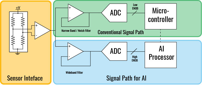 The classic AFE may need to change to accommodate the sensor and digital processing sections, and the AI model’s needs which may be different. (Source: Avnet)
For signals with a wide dynamic range, it may make sense to employ automated gain control (AGC) to ensure there is enough detail in the recorded signal under all practical conditions. The changes in amplification should also be passed to the digitizer and synchronized with the sensor data so they can be recorded as features during AI training or combined by a preprocessing step into higher-resolution samples. If not, the model may learn the wrong features during training.
Interfacing AI systems with multi-sensor designs
Multi-sensor designs introduce another consideration. Devices that process biological signals or industrial condition-monitoring systems often need to process multiple types of data together. Time-synchronized data will deliver the best results as changes in group delay caused by filtering or digitization pipelines of different depths can change the relationship between signals.
The use of AI may lead the designer to make choices they might not make for simpler systems. For example, aggressive low- and high-pass filtering might help deliver signals that are easier for traditional software to interpret. But this filtering may obscure signal features that are useful to the AI.
| Design Tip – Analog Switches & Multiplexers
Analog switches and multiplexers perform an important role in AFEs where multiple sensors are used in the signal chain. Typically, devices are digitally addressed and controlled, switches selectively connect inputs to outputs, while multiplexers route a specific input to a common output. Design considerations include resistance, switching speed, bandwidth, and crosstalk. |
For example, high-pass filtering can be useful for removing apparent signal drift but will also remove cues from low-frequency sources, such as long-term changes in pressure. Low-pass filtering may remove high-frequency signal components, such as transients, that are useful for AI-based interpretation. It may be better to perform the filtering digitally after conversion for other downstream uses of the data.
Techniques for optimizing energy efficiency in AFEs
Programmable AFEs, or interchangeable AFE pipelines, can improve energy optimization. It is common for edge devices to operate in a low-energy “always on” mode, acquiring signals at a relatively low level of accuracy while the AI model is inactive. Once a signal passes a threshold, the system wakes the AI accelerator and moves into a high-accuracy acquisition mode.
That change can be accommodated in some cases by programming the preamplifiers and similar components in the AFE to switch between low-power and low-noise modes dynamically.
A different approach often used in biomedical sensors is to use changes in duty cycles to reduce overall energy. In the low-power state, the AFE may operate at a relatively low data rate and powered down during quiet intervals. The risk arises of the system missing important events. An alternative is to use a separate, low-accuracy AFE circuit that runs at nanowatt levels. This circuitry may be quite different to the main AFE signal path.
In audio sensing, one possibility is to use a frequency-detection circuit coupled with a comparator to listen for specific events captured by a microphone. A basic frequency detector, consisting of a simple bandpass filter and comparator, may wake the system or move the low-power AFE into a second, higher-power state, but not the full wakefulness mode that engages the back-end digital AI model.
In this state, a circuit such as a generalized impedance converter can be manipulated to sweep the frequency range and look for further peaks to see if the incoming signal meets the wakeup criteria. That multistage approach will limit the time during which the full AI model needs to be active.
Breaking down analog front-ends for AI
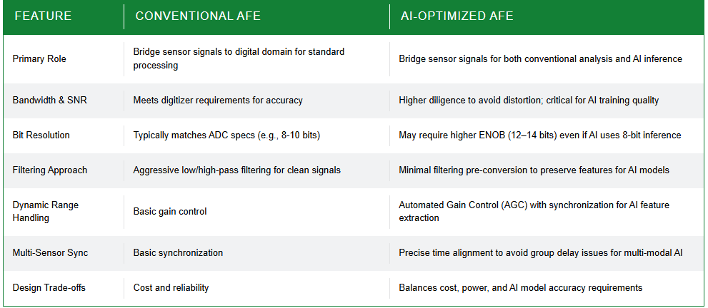
Further advances in AI theory enable more sophisticated analog-domain processing before digitization. Some vendors have specialized in neural-network devices that combine on-chip memory with analog computation. Another possibility for AFE-based AI that results in a lower hardware overhead is reservoir computing. This uses concepts from the theory of recurrent neural networks. A signal fed back into a randomly connected network, known as the reservoir, can act as a discriminator used by an output layer that is trained to recognize certain output states as representing an event of interest. This provides the ability to train an AFE on trigger states that are more complex than simple threshold detectors.
Another method for trading off AFE signal quality against AI capability is compressive or compressed sensing. This uses known signal characteristics, such as sparsity, to lower the sample rate and, with it, power. Though this mainly affects the choice of sampling rate in the analog-to-digital converter, the AFE still needs to be designed to accommodate the signal’s full bandwidth. At the same time, the AFE may need to incorporate stronger front-end filtering to block interferers that may fold into the measurement frequency range.
Optimizing AFE/AI trade-offs through experimentation
With so many choices, experimentation will be key to determining the best tradeoffs for the target system. Operating at higher bandwidth and resolution specifications is a good start. Data can be readily filtered and converted to the digital domain at lower resolutions to see how they affect AI model performance.
The results of those experiments can be used to determine the target AFE’s specifications in terms of gain, filtering, bandwidth, and the ENOB needed. Such experiments also provide opportunities to experiment with more novel AFE processing, such as reservoir computing and compressive sensing to gauge how well they might enhance the final system.
The post Optimized analog front-end design for edge AI appeared first on ELE Times.
Introducing Wi-Fi 8: The Next Boost for the Wireless AI Edge
Courtesy: Broadcom
Wi-Fi 8 has officially arrived—and it marks a major leap forward for next-generation connectivity.
Wi-Fi has come a long way. Earlier generations (Wi-Fi 1 through 5) focused mainly on delivering content to users: streaming video, online gaming, and video calls. But today’s digital world runs in both directions. We create as much data as we consume. We upload high-resolution content, collaborate in real time, and rely on on-device AI for everything from productivity to entertainment. That makes the “last hop” between devices and wireless networks more critical than ever.
Wi-Fi 8 is built for this new reality. Evolving from the advances of Wi-Fi 6 and 7, it offers reliable performance at scale, consistently low latency, and significantly stronger uplink capacity—precisely what modern, AI-driven applications need to run smoothly and responsively.
Why Wi-Fi 8 Matters
The internet has shifted from passive browsing to immersive, interactive, and personalized experiences. Devices now sense, analyze, and generate data constantly. By the end of 2025, hundreds of millions of terabytes will be created every day, much of it from IoT, enterprise telemetry, and video. A lot of that data never even makes it to the cloud—it’s handled locally. But guess what still carries it around? Wi-Fi.
Uplink matters
Traditional traffic patterns skewed roughly 90/10 downlink/uplink. Not anymore. AI apps, smart assistants, and continuous sync push networks toward a 50/50 split. Your Wi-Fi can’t just be fast going to you—it has to be equally fast, fair, and predictable going from you.
Real-time Wi-Fi
In the age of AI, Wi-Fi has to be far more real-time. Take, for example, agentic apps that work with voice inputs. We all know today’s assistants can feel clunky—they buffer, they miss interruptions. To get to your true agentic assistant with a “Jarvis-like” back-and-forth, networks need ultra-low latency, less jitter, and fewer drops.
With the right broadband and Wi-Fi 8, those thresholds become possible.
What’s New in Wi-Fi 8
Wi-Fi 8 delivers a system-wide upgrade across speed, capacity, reach, and reliability. Here’s what that means in practice:

Higher throughput—more of the time: Wi-Fi 8 achieves higher real-world speeds with smarter tools. Unequal Modulation ensures each stream runs at its best rate, so one fading link doesn’t drag the others down. Enhanced MCS smooths out the data-rate ladder to prevent sudden slowdowns, while Advanced LDPC codes hold strong even in noisy conditions. The result: faster, steadier performance across the network.
More network capacity in busy air: In crowded spaces, Wi-Fi 8 is built for cooperation. Inter-AP Coordination helps access points schedule transmissions instead of colliding. Non-Primary Channel Access (NPCA) taps into secondary channels when the primary is congested, while Dynamic Subband Operation (DSO) lets wide channels serve multiple narrower-band clients at once. Dynamic Bandwidth Expansion (DBE) then selectively opens wider pipes for Wi-Fi 8 devices without disrupting legacy clients—unlocking more usable capacity where it’s needed most.
Longer reach and stronger coverage close to the edge: Connections go farther with Distributed Resource Units (dRU), which spread transmit energy for noticeable gains at the fringe. And with Enhanced Long Range (ELR), a special 20-MHz mode extends coverage up to 2× in line-of-sight and about 50% farther in non-LoS—keeping links alive even at the outer edge of the network.
Reliability and QoS that stick: Real-time apps get the consistency they need thanks to smarter quality-of-service features. Low-Latency Indication prioritizes AR/VR, gaming, and voice traffic, while Seamless Roaming keeps calls and streams intact during movement. QoS enhancements and Prioritized EDCA reduce latency and prevent bottlenecks across multiple streams. Plus, enhanced in-device coexistence coordinates Wi-Fi with Bluetooth, UWB, and more to avoid self-interference. Together, these features make the network feel smoother and more reliable.
Wi-Fi 8 Real-World Impact
So what does all this look like in everyday use? Assume a busy apartment building, or an office full of devices roaming between access points. Signals aren’t perfect, interference is everywhere, but Wi-Fi 8 keeps things flowing. It does this by coordinating access points, smoothing out delays, and reducing radio clashes—so your most important traffic doesn’t get stuck in line.
Picture this: It’s a busy evening in a modern family home. One person is streaming a live sports match in 8K on the big screen, another is deep into an online game while streaming to friends, and a third is working on a project that involves real-time AI voice assistance.
Meanwhile, the smart doorbell detects someone approaching. But instead of just pinging a vague “motion alert,” the AI-powered camera recognizes whether it’s a delivery driver dropping off a package, a neighbor stopping by, or a family member arriving home. The alert is contextual and useful.
In older Wi-Fi environments, that mix of high-bandwidth streams, real-time gaming, and constant AI inference could lead to stutters, buffering, or dropped packets at the worst moments. With Wi-Fi 8, all of it just works. The 8K stream stays crisp. The gamer experiences smooth, low-latency play. The AI assistant responds instantly without awkward delays. And the doorbell notification comes through without competing for airtime—because the network can intelligently prioritize, coordinate, and balance all that traffic.
That’s the difference Wi-Fi 8 brings: a reliable home network, no matter how many devices or demands are piled on at once.

Why it works: Wi-Fi 8 increases throughput and, at the same time, greatly reduces the 99th percentile latency tail. By coordinating APs, elevating delayed packets, and reducing radio self-contention, it shortens queues, avoids collisions, and keeps critical traffic flowing—even when signals aren’t perfect.
Conclusion
Wi-Fi 8 represents far more than an incremental upgrade—it marks a fundamental shift in how wireless networks will power the AI-driven world. As our homes, offices, factories, and devices generate and process more data than ever, the need for reliable uplink performance, real-time responsiveness, and intelligent coordination becomes non-negotiable. Broadcom’s new ecosystem brings these capabilities to life, ensuring that next-generation applications—from immersive entertainment and autonomous IoT to true conversational AI—can operate smoothly, consistently, and securely.
With Wi-Fi 8, the wireless edge finally catches up to the ambitions of modern computing. It isn’t just faster Wi-Fi; it’s the foundation for the seamless, AI-enabled experiences we’ve been waiting for—and a major leap toward the connected future we’re building every day.
The post Introducing Wi-Fi 8: The Next Boost for the Wireless AI Edge appeared first on ELE Times.
Vehicle to Grid (V2G) Charging in EVs: Understanding the Basics
Much of the research around emerging technologies in Electric vehicles is looking within the EV system and lack a comprehensive review of EV integration and its impact on Power system planning and operation, across transmission and distribution levels.
Shift Toward Bidirectional Energy Flows
Vehicle to Grid (V2G) charging is a phenomenal step taken in direction of placing EVs on the energy landscape where they can contribute to grid stability. V2G integration provides a paradigm shift from an era of unidirectional energy flow and introduces bidirectional energy transfer between EVs and energy grid. EVs essentially act as renewable energy storage units facilitating load balancing, peak shaving and frequency regulation within the grid.
Core Components of V2G Systems
- EV as Portable Energy Storage: The V2G system primarily consist of EV as a potable energy storage system fitted with a battery management system (BMS).
- EVSE, Chargers and Communication Interfacee: The Electrical vehicle supply equipment (EVSE) is connected to the EV, including a bidirectional charger and a communication interface that allows data flow between EV, grid and the user.
- Supporting Infrastructure: It also integrates a transformer to manage voltage levels, a smart meter for precise monitoring and an aggregator platform for coordination of combined energy sources from many EVs.
Variants of Bidirectional Charging
In addition to V2G, bidirectional energy transfer covers V2H (vehicle-to-home) and V2L (vehicle-to-load) charging.
Global Deployment Landscape
Adoption Examples: Virta Global, is a European country headquartered at Helsinki, Finland that is leading in providing V2G solutions. It has installed seven V2G chargers at its premises in Finland. Virta has installed 20 chargers at a Nissan manufacturing plant in the UK.
Economic Considerations
Battery Cycling and Infrastructure Costs: There are, however, cost considerations to be considered with V2G charging. The batteries in a V2G setup are subject to wear and tear due to frequent charging and discharging cycles. Advance chargers and communication systems add to the cost, even though a part of it is offset by revenue opportunities gained from selling stored energy.
Impact on Power Networks
- Grid Benefits and Load Management: The electrical network is largely benefited by V2G charging during load shifting, load building, power conservation, peak clipping, valley filling and flexible loads. As increasingly EVs get integrated into the system, power imbalances on the load side are bound to occur. The ancillary services provided by the V2G setup help in alleviating certain congestions on the network.
Role of Aggregators and Control Models
Aggregation for Frequency Control: Aggregation of numerous EVs into grid through V2G setup for primary frequency control is a critical to larger EV integration into the transportation system. Aggregators assist in providing services to individual EVs and serve the purpose of a bigger and more appropriate load for utility.
Models Used in Research
Studies are ongoing on several aggregated models for large-scale EV integration. Some researchers use an independent distributed Vehicle to grid regulation arrangement while others use master slaves grid regulation technique for microgrid (MG) in islanding mode.
Modified Droop Controller Approach
However, modified droop controller method is considered better than others where the reference signal is controlled and monitored uninterruptedly by a droop controller possessing feedback mechanism. Such controller is known as Modified droop controller.
Technical Capabilities of V2G Systems
- Active and Reactive Power Support: In V2G system, the vehicle can provide active power regulation, current harmonic filtering, reactive power support and tracing of adjustable renewable energy sources.
- Ancillary Services: With the help of these, ancillary services such as frequency and voltage control can be facilitated.
Microgrid-Level Power Balancing
Optimized Charging Schedules: A better balance of power in a microgrid can be achieved by Vehicle to grid systems. With the help of intelligent charging schedules, the vehicle can discharge during peak hours, charge during off-peak hours, thereby improving the load curve.
Voltage and Frequency Regulation
Up and Down Regulation
Regulation of voltage and primary frequency are crucial for energy markets. When the voltage supply from the grid is high, the EV battery is in charging state known as down regulation. On the contrary, when supply from the grid is low, EV battery is in discharging state also known as up regulation. This may affect the frequency. The primary purpose of frequency control is to maintain equilibrium between generation and demand within specific time duration. Regulation services can be provided within V2G systems to reduce pressure on the power grid.
Harmonic Filtration and Power Quality
Need for Harmonic Control: Maintaining the quality of power supplied back to the grid through Harmonic filtration is essential for any emerging V2G technology.
Advances in Digital IIR Filters: Recently, real-time digital infinite impulse response (IIR) filters are developed for the same. IIR filters generate reference signals at the power calculation stage. Digital filters offer various advantages over passive and active filters in inverter output signals of V2G applications like real-time processing, adaptability, improved performance with better noise reduction, increased control and lower costs.
V2G Applications in Fuel-Cell EVs
IIR Filters in FCEVs: Digital IIR filters are mostly implemented in Fuel Cell Electric vehicles (FCEVs) because they require less memory and have less computational complexity.
Global Research Initiatives
The European Union’s Hydrogen Mobility Europe 2 (H2ME2) project is researching and developing V2G technology for FCEVs to demonstrate the technology in a real-world setting. Other companies, such as Toyota and Hyundai, have also announced plans to develop V2G technology for their FCEVs. Moreover, companies like Texas instruments are researching on application of digital IIR filters.
Conclusion: EVs as Grid Assets
Electric vehicles can act both as a load and a potential power source which can be integrated into the power system when required. Adequate studies on the stresses that a power distribution system can experience due to large scale EV adoption are imperative and equally imperative is to come up with alternatives like V2G technology that can overcome some of these challenges.
The post Vehicle to Grid (V2G) Charging in EVs: Understanding the Basics appeared first on ELE Times.
ROHM launches SiC MOSFETs in TOLL package that achieves both miniaturization and high-power capability
ROHM has begun mass production of the SCT40xxDLL series of SiC MOSFETs in TOLL (TO-Leadless) packages. Compared to conventional packages (TO-263-7L) with equivalent voltage ratings and on-resistance, these new packages offer approximately 39% improved thermal performance. This enables high-power handling despite their compact size and low profile. It is ideal for industrial equipment such as server power supplies and ESS (Energy Storage Systems) where the power density is increasing, and low-profile components are required to enable miniaturized product design.
In applications like AI servers and compact PV inverters, the trend toward higher power ratings is occurring simultaneously with the contradictory demand for miniaturization, requiring power MOSFETs to achieve higher power density. Particularly in totem pole PFC circuits for slim power supplies, often called “the pizza box type,” stringent requirements demand thicknesses of 4mm or less for discrete semiconductors.
ROHM’s new product addresses these needs by reducing component footprint by approximately 26% and achieving a low profile of 2.3mm thickness – roughly half that of conventional packaged products. Furthermore, while most standard TOLL package products are limited by a drain-source rated voltage of 650V, ROHM’s new products support up to 750V. This allows for lower gate resistance and increased safety margin for surge voltages, contributing to reduced switching losses.
The lineup consists of six models with on-resistance ranging from 13mΩ to 65mΩ, with mass production started in September 2025 (sample price: $37.0/unit, tax excluded). These products are available for online purchase from online distributors such as DigiKey, MOUSER, and Farnell. Simulation models for all six new products are available on ROHM’s official website, supporting rapid circuit design evaluation.
Product Lineup
Application Examples
・Industrial equipment: Power supplies for AI servers and data centers, PV inverters, ESS (energy storage systems)
・Consumer equipment: General power supplies
The post ROHM launches SiC MOSFETs in TOLL package that achieves both miniaturization and high-power capability appeared first on ELE Times.
Сторінки

