
ELE Times

Dell Technologies’ 2026 Predictions: AI Acceleration, Sovereign AI & Governance
Dell Technologies hosted its Predictions: 2026 & Beyond briefing for the Asia Pacific Japan & Greater China (APJC) media, where the company’s Global Chief Technology Officer & Chief AI Officer, John Roese, and APJC President, Peter Marrs, outlined the transformative technology trends and Dell’s strategies for accelerating AI adoption and innovation in the region.
 John Roese’s vision on the trends set to shape the technology industry in 2026 and beyond (Image Credits: Dell Technologies)
According to Roese, the rapid acceleration of AI is set to profoundly reengineer the entire fabric of enterprise and industry, driving new ways of operating, building, and innovating at an unprecedented scale and pace.
Focus on scalability and real adoption
A key trend is the shift in focus towards scaling AI for tangible business outcomes. “Conversations are on very real adoption, and AI is creating a truly transformational opportunity,” said Marrs. “We are working with customers across the region to build AI at scale.”
Marrs noted that growing deployment of agentic AI is an example of this transformation, with organizations such as Zoho in India already working with Dell to accelerate agentic AI adoption by delivering contextual, privacy-first and multimodal enterprise AI solutions. “AI has become more accessible for all companies in the region, and what we’ve been doing is successfully building foundations with customers to deploy AI at scale.”
Roese highlighted that the industry is now entering the autonomous agent era, where agentic AI is evolving from a helpful assistant to an integral manager of complex, long-running processes. “We expect that as people go on the agentic journey into 2026, they will be surprised by how much more agents do for them than they anticipated. Its very presence will bring value to make humans more efficient, and make the non-AI work, work better,” he noted.
As the industry continues to build and deploy more enterprise AI, Roese also emphasized the need for businesses to rethink how they treat and make resilient AI factories.
Sovereign AI and governance as the foundation for innovation
With the light-speed acceleration of AI development, there is a degree of volatility. Roese predicted that the demand for robust governance frameworks and private, controlled AI environments will become undeniable, urging the industry to build on both internal and external AI guardrails that allow organizations to innovate safely and sustainably.
“Last year, we predicted that ‘Agentic’ would be the word of 2025. This year, the word ‘Governance’ is going to play a much bigger role,” Roese said. “The technology and its use cases are not going to be successful if you do not have discipline and governance around how you operate your AI strategy as either an enterprise, a region, or a country.”
At national levels, the rapid rise of sovereign AI ecosystems will continue as AI becomes critical to state-level interests. Marrs discussed this trend’s momentum, noting that like many countries in the region, enterprises are also actively building their own frameworks to drive local innovation, with strong foundations already in place.
Building the ecosystem for impact and progress
To bridge that gap, Marrs reiterated the importance of a collaborative ecosystem in nurturing a skilled talent pool and advancing the region’s AI competitiveness, citing the APJ AI Innovation Hub as an initiative that is delivering impact through the combination of Dell’s capabilities, talent, and ecosystem.
“By working with experts, government, and industry peers, we’ve made unbelievable headway in fostering skill development and advancing our collective expertise,” said Marrs. “Together, we are accelerating Asia’s leadership as an AI region, identifying key steps to bolster the region’s growth. Dell is excited about how we’re participating and helping with this transformation.”
The post Dell Technologies’ 2026 Predictions: AI Acceleration, Sovereign AI & Governance appeared first on ELE Times.
NAL-CSIR Advances Field testing of Indigenous Defence Tech
The Council of Scientific and Industrial Research (CSIR)-National Aerospace Laboratories (NAL), in collaboration with Solar Defence & Aerospace Ltd. (SDAL), a private industry partner co-developed a 150-kg class Loitering Munition UAV (LM-UAV).
The drone system has an indigenous Wankel engine which is a perfect blend of efficiency and reliability, essential for defence products. With an operational range of up to 900 kilometres and an endurance for 6-9 hours, the drone is reliable for long missions. The system also has an operability at service ceilings reaching 5 kilometres which ensures altitude flexibility. The system is fitted with cutting edge features, such as GPS-denied navigation, essential for situations where the GPS is compromised, along with a low-radar cross-section that enhances its stealth characteristics.
The drone system is also updated with latest AI technology for target identification which will boost precision and autonomy during missions.
Next, is the field testing for High Altitude Platforms (HAPs), a solar-powered unmanned aircraft, capable of a sustained flight above a 20-kilometre altitude. These HAPs act as pseudo-satellites, used for extended surveillance, communication, and reconnaissance purposes.
The field testing of the 150-kg class LM-UAV and the development of solar-powered HAPs mark important milestones in India’s evolving indigenous defence technology landscape. These advancements are testament to the country’s commitment to building resilient and self-sustaining defence assets through collaborative public-private partnerships and cutting-edge aerospace research.
They are part of India’s efforts to develop self-reliant defence technologies under the ‘Atmanirbhar Bharat’ Initiative.
The post NAL-CSIR Advances Field testing of Indigenous Defence Tech appeared first on ELE Times.
Toyota & NISE Test Mirai Hydrogen FCEV in India Conditions
Toyota Kirloskar Motor (TKM) and the National Institute of Solar Energy (NISE) under the Ministry of New and Renewable Energy signed an MoU to collaborate to test Toyota’s Mirai, a hydrogen fuel-celled EV in Indian conditions.
The MoU was signed in the presence of Union Minister of New and Renewable Energy and Consumer Affairs, Food and Public Distribution, Prahlad Joshi in New Delhi. Under the said agreement, Toyota has handed over its Toyota Mirai to NISE who will conduct a comprehensive real-world test on the vehicle. The study will judge Mirai’s performance across Indian climates, terrains, and driving conditions.
NISE will study the fuel efficiency, real-world range, refuelling patterns, drivability, environmental resilience, along with the overall adaptability of the vehicle to Indian roads and traffic conditions. These results are then expected to manoeuvre the early-stage adoption of hydrogen mobility technologies in the country.
This initiative will be a breakthrough in the advancement for Hydrogen mobility in the country. It will also support India’s Green Hydrogen Mission and strengthen the country’s decarbonisation and clean transportation goals.
India’s decarbonization goals revolve around its Panchamrit targets: reaching 500 GW non-fossil fuel capacity and 50% renewable energy by 2030, cutting emissions intensity by 45% (vs. 2005) and reducing total emissions by 1 billion tonnes by 2030, all leading to Net-Zero by 2070, driven by massive solar, wind, green hydrogen, battery storage, and grid improvements.
The post Toyota & NISE Test Mirai Hydrogen FCEV in India Conditions appeared first on ELE Times.
Nissan Powering EV Component Plant with Repurposed Batteries
Nissan Australia has launched the Nissan Node project, a circular economy initiative which will repurpose end-of-life Nissan Leaf batteries to power a section of its Dandenong production facility.
This initiative is part of Nissan’s sustainability strategy. The project involves the installation of a new solar array along with a battery-energy storage system, made from repurposed first-generation Leaf batteries at the Nissan Casting Australia Plant (NCAP).
EV manufacturing is said to have a 50-100% higher production emission as compared to ICE vehicles due to battery manufacturing.
Nissan expects its new system to cut NCAP’s annual CO2 emissions by nearly 259 tonnes while saving approximately 128 megawatt-hours of energy annually.
“This isn’t just a hugely exciting project, but an important step into the future for end-of-life EV batteries,” Nissan Oceania managing director Andrew Humberstone says.
“As an early pioneer of the electric vehicle both globally and locally, we can also demonstrate leadership in second-life battery initiatives. I’m proud that this solution is every bit as innovative as the launch of not only the Leaf but the recently introduced ARIYA.”
The initiative was delivered in partnership with Melbourne-based technology firm Relectrify, which developed the battery-management and inverter technology enabling second-life Leaf batteries to be repurposed effectively. Its ReVolve energy-storage system installed at NCAP is the first commercial product built entirely from retired Leaf batteries.
The post Nissan Powering EV Component Plant with Repurposed Batteries appeared first on ELE Times.
KEC, Powernet & Wise Integration Co-Develop AI Server SMPS Power Solutions
Wise Integration (France), Powernet (Korea) and KEC (Korea) will co-develop next-generation switched-mode power supply (SMPS) solutions designed specifically for AI server applications in South Korea. The partnership aligns with the country’s push to expand AI infrastructure and build out the next generation of high-density data centers.
Under the agreement, Wise Integration will supply its GaN (gallium-nitride) power devices, digital-control expertise and technical support. Powernet Technologies Corporation will lead development of new SMPS designs using Wise’s WiseGan and WiseWare technologies. KEC Corporation will manage backend manufacturing, including module integration and system-in-package production tailored to the thermal and reliability demands of AI-server racks.
In addition to accelerating the design and development of competitive AI-server power supply solutions and creating business opportunities in Korea’s AI server market, the project aims to shorten the solutions’ time-to-market using WiseGan and WiseWare technologies. The collaboration builds on an earlier partnership between Wise Integration and Powernet, launched to serve OEMs that require compact, digitally controlled power-supply systems for faster, smaller and more energy-efficient electronic equipment.
AI servers draw extensive power, generate intense heat, and depend on SMPS designs capable of converting high-voltage input (e.g., 400 V) to stable 48 V rails with minimal loss. GaN devices with digital control are uniquely suited for that task: they enable higher switching frequencies, greater efficiency, and more precise management of fast, high-current load transients.
Supporting South Korea’s National Ambition
The South Korean government’s investments in AI-dedicated data centers includes high-performance GPU clusters and digital infrastructure that supports demand for more efficient, compact, and scalable power-conversion systems.
“Korea is moving quickly to build the next generation of AI data centers, and power architecture is a critical piece of that effort. Working with Powernet and KEC lets us bring GaN-based digital control into server-grade designs at scale—delivering the efficiency, thermal performance, and responsiveness that modern AI hardware depends on,” said Ghislain Kaiser, CEO of Wise Integration.
Technology Momentum: A Logical Extension of Wise Integration’s Roadmap
Beyond the MoU, Wise Integration has been widening the foundation that supports strategic partnerships. As Korea accelerates AI-ready data-center development, the demands on power-conversion systems intensify—higher switching frequencies, tighter thermal budgets and more aggressive efficiency targets. Wise has been expanding its GaN + digital-control portfolio to meet those constraints, ensuring the technologies Korea aims to deploy at scale already have a maturing, production-validated base behind them.
For example, the company recently launched WiseWare 1.0 for totem-pole PFC and LLC topologies, its newest fully digital controller. While aimed today at gaming, displays and industrial systems, it shares the same architecture—high-frequency GaN operation, compact form factor, digitally managed efficiency—that naturally scales into the server-class designs targeted under the Korea-focused collaboration.
The post KEC, Powernet & Wise Integration Co-Develop AI Server SMPS Power Solutions appeared first on ELE Times.
FAMES Pilot Line R&D Advances: 400°C CMOS Enables 3D Integration Goals
CEA-Leti, the coordinator of the FAMES Pilot line, has achieved a major milestone for next-generation chip stacking: fully functional 2.5 V SOI CMOS devices fabricated at 400°C. The devices match electrical performance of devices fabricated at standard thermal budget (>1000 °C), removing one of the last barriers to large-scale 3D sequential integration (3DSI) —a core objective of FAMES.
Enabled by advanced CEA-Leti expertise in low-temperature processes (nanosecond laser annealing (NLA) and solid-phase epitaxy regrowth (SPER)), this work offers true three-dimensional device stacking from the lab to fab. 3D sequential-integration interconnection density between tiers is the highest among 3D technologies, such as TSV and hybrid bonding. In this project, CEA-Leti demonstrated that Si CMOS is BEOL compatible, and thus can be stacked safely above BEOL, while transistor performance and maturity overtake largely the other technological options from the state-of-the-art, low-temperature solutions.
The achievement, presented today in a paper at IEDM 2025, titled, “High Performance 2.5 V n&p 400 °C SOI MOSFETs: A Breakthrough for Versatile 3D Sequential Integration,” is a key breakthrough for the FAMES Pilot Line, a European Union initiative launched in 2023 in response to the EU Chips Act strategy to strengthen sovereignty and competitiveness in semiconductor technologies. By combining 3D heterogeneous and sequential integration on FD-SOI platforms, the consortium aims to enable a new generation of More-Than-Moore devices and applications.
Enabling New Chip Architectures
“This breakthrough is a major milestone of the FAMES project as it enables innovative new chip architectures,” said Dominique Noguet, CEA-Leti vice president and coordinator of the FAMES Pilot Line. “Our low-temperature process could accelerate real-world demonstrations of multi-tier stacks combining advanced CMOS logic, with smart pixel or RF layers, to create new high-performance 3D chips.”
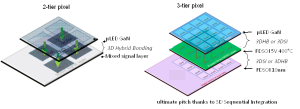 Concept of 3-tier µLED GaN pixel allowing an emissive array with strong pitch reduction thanks to 3DSI in combination with 3D hybrid bonding technology. CEA-Leti’s 400 °C CMOS process enables such top-tier integration without exceeding the thermal limits of the active circuitry below.
The team showed that SOI devices processed at 400 °C instead of the high temperature (>1000 °C) industry standard and high-temperature industrial reference, performed equivalent to high-temperature devices.
“The 400 °C process enables 3D sequential stacking on any bottom tier,” Noguet said. “It’s a huge step forward because it’s far more mature—reliable and scalable—than current low-temperature solutions, such as polycrystalline films, oxide semiconductors or carbon nanotubes.”
Protecting Circuitry on Bottom-Tier LayersCEA-Leti’s team demonstrated n- and p-type transistors matching the characteristics of conventional high-temperature CMOS devices, while staying within the ≤400 °C thermal budget required to preserve active circuitry in lower layers.
The process relies on an optimized 400 °C LPCVD deposition for amorphous silicon followed by NLA in the melt regime for dopant activation and diffusion—producing polycrystalline, low-resistance gates with excellent interface quality. In addition, NLA-SPER mastering enables dopant activation without diffusion leading to access resistance within specifications.
The post FAMES Pilot Line R&D Advances: 400°C CMOS Enables 3D Integration Goals appeared first on ELE Times.
Keysight & KT SAT Nail Industry First GEO-to-LEO Multi-Orbit NTN Handover!
Keysight Technologies, Inc., in collaboration with KT SAT, has demonstrated a successful non-terrestrial network (NTN) handover using the KOREASAT-6A satellite at KT SAT’s Kumsan Satellite Network Operation Center in Korea. In a controlled clinical environment, the companies established the industry’s first NR-NTN multi-orbit handover between a commercial GEO satellite and an emulated LEO link. The demonstration was performed over a live Ku‑band GEO connection (DL ~12.3 GHz / UL ~14.4 GHz), marking a major milestone toward testing the newly standardized 3GPP Rel‑19 Ku‑band NTN spectrum. By incorporating Ku‑band operation into this multi-orbit mobility scenario, Keysight and KT SAT have validated NTN behaviors in a frequency range now central to emerging global standards and operator deployment strategies.
As the industry moves toward 6G, integrating satellite and terrestrial networks is essential to deliver continuous coverage and resilient service in remote or disaster-affected areas. Satellite links, however, introduce longer delays, Doppler effects, and dynamic link conditions that complicate mobility and handover across space and ground domains.
By moving beyond earlier demonstrations focused on single-orbit GEO connectivity, KT SAT and Keysight have shown how operators can evolve from point-to-point satellite links to continuous multi-orbit mobility, expanding KT SAT’s service capabilities toward resilient, always-on coverage across space and ground domains. This achievement also establishes an important technical milestone for KT SAT and Keysight in advancing Ku-band NTN mobility.
Using Keysight’s Network Emulator Solutions and UeSIM RAN Testing Toolset, the teams emulated the base station and user equipment, established a two-way link through KOREASAT-6A, and maintained service continuity during a handover from GEO to an emulated LEO connection. Operating the GEO link in Ku‑band ensures that these mobility insights directly map to the Rel‑19 NTN frequency bands now entering commercial planning, giving operators and device vendors earlier visibility into real‑world propagation, timing, and interoperability behaviors. As a result, KT SAT can now explore and validate advanced NTN mobility scenarios in the lab, before satellites or user devices are widely deployed, accelerating its roadmap and reducing the time and cost of bringing new multi-orbit services to market.
This collaboration shows how operators can extend coverage and resilience, while device and chipset vendors gain a lab-based path to validate NTN mobility without relying solely on expensive field trials. Insights from this work are intended to inform standards discussions and operator evaluations, helping the ecosystem shorten time-to-trial and de-risk commercialization.
Seo Young-soo, CEO of KT SAT, said: “As the only satellite communications service provider in Korea, KT SAT is progressively validating the applicability of NTN gNB and UE using our five operational GEO satellites. Building on the results of this trial, we will actively explore strengthening the competitiveness of our next-generation GEO satellite for the global market and delivering integrated multi-orbit communication services based on NTN systems, including traffic handover across our own GEO and future LEO/MEO constellations.”
Peng Cao, Vice President and General Manager of Keysight’s Wireless Test Group, Keysight, said: “This demonstration shows how emulation can bring future multi-orbit networks into the lab today. By combining a live GEO connection with emulated LEO conditions using NR-NTN parameters in Ku-band, Keysight gives operators and vendors a practical way to study NTN handover behavior, optimize mobility strategies, and reduce the cost and risk of early deployments.”
The post Keysight & KT SAT Nail Industry First GEO-to-LEO Multi-Orbit NTN Handover! appeared first on ELE Times.
Nuvoton Emphasises Need to Strengthen Taiwan-Israel R&D Collaboration
Nuvoton Technology showcased its leadership in international expansion by participating in the “Israeli-Taiwanese Business Seminar,” hosted by the Economic Division of the Taipei Economic and Cultural Office in Tel Aviv from November 15 to 23. Drawing attention to the practical advantages of its established R&D center in Israel, Nuvoton played a key role in the seminar, sharing on-the-ground insights from its cross-border expansion.
Nuvoton stated that investments in global hubs such as Israel are not only an expansion of its business footprint but also a critical part of its long-term development strategy. By connecting innovation talent and technology networks worldwide, Nuvoton aims to address emerging market challenges and opportunities while helping build a more resilient and competitive Taiwan-Israel technology ecosystem.
During the seminar, Nuvoton highlighted opportunities for collaboration in R&D, technology, and market development among global enterprises. The company’s practical experience offered the delegation concrete guidance for establishing operations in Israel and accessing its innovation resources, reflecting the collaborative spirit within Taiwan’s technology community.
Nuvoton emphasized the complementary strengths of Taiwan and Israel in the high-tech sector: Taiwan excels in IC designing, while Israel leads in software innovation. Building on these advantages, Nuvoton has accelerated its global R&D strategy by establishing an R&D center in Israel, enabling the company to strengthen its international competitiveness.
The post Nuvoton Emphasises Need to Strengthen Taiwan-Israel R&D Collaboration appeared first on ELE Times.
element 14’s DevKit HQ: A One Stop Development Kit Solution
Engineering is all about trying and testing. According to a survey conducted by element 14, most engineering professionals feel that finding the right development kit is a major challenge. Identifying a holistic development kit is essential for most engineers before starting a project. They value standard interfaces and extensibility, often combining or modifying multiple kits to build prototypes and proof-of-concept designs.
Element 14 has come forward with DevKit HQ, a new online resource that brings evaluation boards, development kits, single board computers (SBCs), tools, and technical documents, all in one place. DevKit HQ brings together resources from key supplier product families, like Analog Devices, NXP, AMD, STMicroelectronics, Microchip, Infineon, Renesas, Raspberry Pi, BeagleBoard, Arduino, and more, for multiple purposes, such as, AI/ML, IoT, sensors, wireless, motor control, and power management. This makes it easy for developers to discover, compare, and accelerate their embedded design and innovation.
The site enables engineers to quickly find the latest development kits and modular solutions by application, along with available demo and application software. Engineers can also easily locate evaluation boards that match a supplier’s product family or series.
Additionally, the site features each kit’s datasheets, application notes, training videos, reference designs and more. Together, these resources help engineers accelerate design decisions and drive innovation across various applications, including AI, IoT, sensors, wireless, motor control and power management.
“Our mission is to make life easier for design engineers,” said Daniel Ford, Vice President of Sales at element14. “With the DevKit HQ, we’ve created the leading destination where they can search development kits by application as well as explore new technologies, experiment with the latest kits, and move from idea to prototype faster, freeing up more time to focus on innovation.’’
The post element 14’s DevKit HQ: A One Stop Development Kit Solution appeared first on ELE Times.
USB-IF Hardware Certification to Anritsu for USB4 2.0 Test Solution
ANRITSU CORPORATION gets certified by the USB Implementers Forum (USB-IF) for its test solution for the latest USB4 Version 2.0 (USB4 v2) communication standard.
The solution is based on the Signal Quality Analyzer-R MP1900A and provides advanced USB device evaluation capabilities. It helps improve the quality and reliability of products implementing the USB4 Version 2.0 standard, supporting widespread deployment of next-generation high-speed interfaces.
As of December 2025, USB4 v2 is the most advanced USB standard, delivering data transfer speeds of up to 80 Gbit/s — twice that of USB4 v1 (40 Gbit/s). This supports next-generation applications, such as high-resolution video transmission, external GPUs, high-speed storage, and VR/AR devices.
Furthermore, the specification significantly improves communication performance and reliability. By introducing innovations including Pulse Amplitude Modulation 3-level (PAM3) signaling to improve bandwidth efficiency, the Frequency Variation Profile to enhance the stability of link training — a signal quality and initialization procedure — and a new TS2.CLKSW training sequence incorporating clock switching.
Current demand for evaluation and certification testing is driven primarily by semiconductor manufacturers producing USB4 v2 control ICs. Looking ahead, adoption is expected to expand to test houses for test equipment deployment and, in the long term, to consumer product manufacturers of USB4 v2 hubs, docking stations, and cables.
Product Overview: Signal Quality Analyzer-R MP1900A
The MP1900A is a high-performance Bit Error Rate Tester (BERT) supporting receiver tests for multiple high-speed interfaces, including PCIe, USB, Thunderbolt, DisplayPort, and 400 GbE/800 GbE. It combines industry-leading PPG technology for high-quality waveforms with a high-sensitivity error detector, precision jitter sources (SJ, RJ, SSC, BUJ), and noise sources (CM-I, DM-I). The MP1900A also supports link training and LTSSM analysis for comprehensive high-speed device evaluation.
The post USB-IF Hardware Certification to Anritsu for USB4 2.0 Test Solution appeared first on ELE Times.
As Energy-Efficient Chips Are Rising — HCLTech × Dolphin’s New Partnership Gives the Trend a Heavy Push
Amid the ongoing push, HCLTech & Dolphin Semiconductors have announced a strategic partnership aiming to develop energy-efficient chips for IoT and data centre applications. As the world moves towards energy-efficient chips, it becomes more imperative than ever to trace the lines that are destined to become the future trends of the industry, at large. When chips come into the picture, energy efficiency is the most organic issue to crop up as it decides the longevity and reliability of the concerned chip. As per the statement by HCLTech and Dolphin Semiconductors, the partnership aims to support enterprises seeking to improve energy efficiency and performance as computing workloads increase.
What are Energy-Efficient Chips?
Energy-efficient chips are integrated circuits designed to perform computations while minimizing power consumption to extend battery life, reduce heat generation, and also lower the operational costs. Its architecture includes specialized cores, such as Neural Processing Units (NPUs) and Graphics Processing Units (GPUs), or, more broadly, AI accelerators rather than conventional CPUs. This is to ensure that tasks are performed using the most efficient hardware possible.
Why is it important?
The proliferation and development of energy-efficient chips is primarily important because, as the usage increases, the power consumption would also increase, and in that case, it is important and indispensable to cut the power requirement and bring the hardware to optimum performance, keeping in mind the sustainability and operation limitations, as the power needed would affect the environment and also cost money simultaneously.
HCLTech X Dolphin Semiconductors Partnership
HCLTech will integrate Dolphin Semiconductor’s low-power IP directly into its SoC design workflow, creating scalable, energy-efficient chips that handle a wide range of compute needs while keeping power use in check.
At its core, energy efficiency requires a holistic, full-stack design effort — from initial architecture to the software that ultimately runs on the chip.
The post As Energy-Efficient Chips Are Rising — HCLTech × Dolphin’s New Partnership Gives the Trend a Heavy Push appeared first on ELE Times.
Advanced GAA Chips: Minimizing Voltage Loss and Improving Yield
Courtesy: Lam Research
- As advanced logic chips decrease in size, voltage loss can increase
- An emerging solution is backside power delivery networks that use SABC architecture
The problem: As metal pitch scaling shrinks to support the next generation of logic devices, the IR (or voltage) drop from conventional frontside connections has become a major challenge.
As electricity travels through a chip’s metal wiring, some voltage gets lost because wires have resistance.
- If the voltage drops too much, the chip’s transistors can’t get enough power and can slow down or fail.
- In addition, the resistance of back-end-of-line (BEOL) metal lines and vias is dramatically increasing.
The solution: Backside power delivery networks (BSPDN) can address these challenges and are currently widely studied as an alternative to front-side power delivery and contact schemes.
Virtual Study Compares DBC and SABC on a GAA Device
The Semiverse Solutions team conducted a virtual study using SEMulator3D to analyze gate-all-around (GAA) devices that use BSPDN.
In the Design of Experiments (DOE), the team focused on a process window for a GAA device that uses a direct backside contact (DBC) architecture and compared it to a GAA device process window using self-aligned backside contact (SABC) architecture.
DBC architecture, used to connect contacts with source/drain structures, requires a deep silicon etch, a small edge placement error (EPE), and precise alignment when used in an advanced GAA transistor.
The Semiverse Solutions team conducted the virtual experiment to see if an SABC scheme could address these precise alignment challenges.
Analyzing the process window of a device helps engineers and researchers understand the range of manufacturing conditions under which a device can be reliably produced while meeting its performance and quality requirements.
By comparing the process windows of different architectures, researchers can identify which design offers greater tolerance to manufacturing variations, fewer defects, and better overall performance.
Figure 1 displays the major integration (process) steps for a proposed SABC scheme. The process steps are like those used during a typical GAA logic process manufacturing flow.
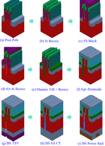 Figure 1. The manufacturing process flow of a proposed self-aligned backside contact (SABC) scheme
Study Methodology
The team ran multiple virtual fabrication experiments that varied the smallest critical dimensions (CD), overlay, and over-etch amount of the through-silicon via (TSV).
Virtual measurements were taken of the number of opens and shorts generated (number of nets in the structure), high-k damage (high-k material volume change), and the backside contact area of the typical structure.
The manufacturing success criteria were specified as follows:
- Backside contact area (CT to epitaxy): ≥150 nm2
- High K damage: <20 nm3
- No contact with the metal gate shorts
Using these criteria, the results of each virtual experiment in the DOE were classified as a “pass” or “failure” event.
SABC Indicates Higher Yield for Advanced Logic Nodes
The DOE results are shown in Figure 2 as a set of process window contour diagrams at various CD, overlay, and over-etch amounts for both the SABC and DBC contact schemes. The green areas in Figure 2 represent “pass” results, while the red areas represent “fail” events.
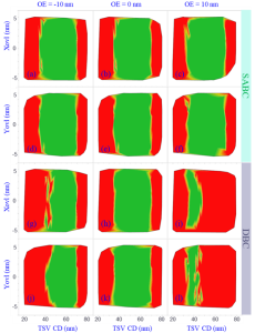 Figure 2. Comparison of SABC and DBC process windows
Due to its self-aligned capabilities, the SABC approach exhibits a much larger process window (larger green area) than the DBC architecture.
The DBC process window is very narrow, especially when the TSV is 10 nm over- or under-etched. The TSV failure exhibits itself as high-k damage, source-drain to metal gate shorts caused by excessive over-etching, small contact areas created by TSV under-etch and increased EPE caused by a larger TSV CD and additional overlay errors.
The virtual study demonstrated that the SABC approach to backside power minimizes EPE and over-etch variations in the TSV process and provides a much larger and more stable process window than a DBC approach. SABC is promising for use at advanced logic nodes and may support further logic device scaling.
The post Advanced GAA Chips: Minimizing Voltage Loss and Improving Yield appeared first on ELE Times.
The Leading Five Essential Context Window Concepts In LLMs
Courtesy: Micron
This story outlines five essential concepts that explain how large language models process input within a context window. Using clear examples and practical insights, it covers foundational ideas like tokenization, sequence length, and attention. The goal is to help readers better understand how context affects model behavior in AI applications. We also present results from an analytical model used to estimate system behavior, to show how scaling input and output sequence lengths impacts response time. The results highlight how decoding longer outputs takes significantly more time, pointing to the importance of fast memory systems like HBM in supporting efficient inference at scale. These concepts are useful for anyone working with or designing prompts for generative AI systems.
Context window versus length
When working with large language models, it’s important to understand the difference between concepts like context window, context length, and sequence length. These terms are often used interchangeably, which can lead to confusion. In this blog, we will define and refer to them as distinct concepts.
The context window is the model’s maximum capacity: the total number of tokens it can process at once, including both your input and the model’s output. As a simple example, let’s define the rectangle size below as equivalent to a 100,000 token context window.
The context length, on the other hand, is how much you’ve put into that space, which is the actual number of tokens—input tokens (blue) and output tokens (green)—currently in use during a conversation. For example, if a model has a 100,000-token context window and your input uses 75,000 tokens, only 25,000 tokens remain for the model’s response before it reaches the upper limit of the window.
Sequence length typically refers to the length of a single input or output sequence within that window. It’s a more granular measure used in model training and inference to track the length of each segment of text.
The context window sets the limit for how much information a model can process, but it does not directly reflect intelligence. A larger window allows more input, yet the quality of the output often depends on how well that input is structured and used. Once the window is full, the model may lose coherence, leading to unwanted outcomes (for example, hallucinations).
Tokens aren’t words
If the context window is defined by an upper limit (say 100,000), tokens are the units that measure what fits inside, and it’s important to understand that tokens are not words. The words you type into a prompt are fed to a “tokenizer,” which breaks down text into tokens. A single word may be split into several tokens. For example, “strawberry” becomes three tokens and “trifle” becomes two. In other cases, a word may consist of just one token, like “cake”.
| St | raw | berry |
We can test this with a quote from the novel “Emma” by Jane Austen.
“Seldom, very seldom, does complete truth belong to any human disclosure; seldom can it happen that something is not a little disguised or a little mistaken.”
This text contains 26 words, and when run through the tokenizer of the Mistral language model provided by lunary.ai1, it produces 36 tokens. That’s about 0.72 words per token or roughly three-fourths of a word.
The ratio varies, but for English words, you might average around 0.75 words per token. That’s why a model with a 100,000-token context window (per user) does not necessarily fit 100,000 words. In practice, you might fit closer to 75,000 English words or fewer, depending on the text.
estimatedtokens≈words∗1.33
To further check the token-to-word ratio at scale, we ran a quick analysis using eight well-known literary works from Project Gutenberg, a library of more than 75,000 free e-books. First, we counted the words in each book, then ran the texts through a tokenizer to get the token counts. After comparing the numbers, we found that the average ratio was about 0.75 words per token.
Knowing this ratio can help everyday users get more out of their interactions with AI. Most AI platforms, like ChatGPT or Claude, operate with token-based constraints. That is, they process text in tokens, not words, so it’s easy to misjudge how much content you can actually fit into a prompt or response. Because usage is often measured in tokens rather than words, knowing the ratio makes you aware of any limits so you can plan your inputs more strategically. For example, if a model has a 4,000-token input limit, that’s roughly 3,000 words. This is good to know when feeding a model a long document or dataset for tasks like finding key insights or answering questions.
Attention is not equally distributed within the context window
AI hallucinations are often misunderstood as quirky behavior or signs that a language model is buggy and unreliable. But hallucinations are not random; they often stem from how a model might process and prioritize information, which is determined by things like how well a model is trained and how it distributes attention. In transformer-based models like GPT or Claude, attention is the mechanism that helps the model decide which parts of the context are most relevant when generating a response. To better understand the concept of attention, imagine being at a noisy cocktail party. If someone calls your name, you instinctively tune in.
“Frodo! Over here!”
But what if four people call your name at once from different corners of the room?
“Frodo! It’s me, Sam!”
“Frodo! Come quick!”
“Frodo! Look this way.”
“Frodo … yesss, precious Frodo …”
You hear them all, but your focus is now split. You might even pay more attention to the voice you recognize or the one closest to you. Each sound gets a fraction of your attention, but not all equally. It’s not a perfect analogy but this is one way you can conceive of how attention works in large language models. The model pays attention to all tokens in the context window, but it gives more weight to some than to others. And that’s why attention in large language models is often described as “weighted”, meaning that not all tokens are treated equally. This uneven distribution is key to understanding how models might prioritize information and why they sometimes appear to lose focus.
More context may or may not mean better answers
A model can scan all tokens within the context window, but it doesn’t consider each token with equal interest. As the window fills (say, up to 100,000 tokens), the model’s attention becomes more diffuse. In its attempt to keep track of everything, clarity may diminish.
When this happens, the model’s grip on the conversation loosens, and a user might experience slower, less coherent responses or confusion between earlier and later parts of the conversation thread. Hallucinations, from the Latin hallucinat or “gone astray in thought,” often appear at this edge. It’s important to understand that these occurrences are not signs that the model is malfunctioning. It is actually an indication that the model is reaching its threshold, where it is operating at capacity. And here is where the model may struggle to maintain coherence or relevance across long spans of input.
From the model’s perspective, earlier tokens are still visible. But as the window fills up and its attention becomes more distributed, the precision of response may degrade. The model might misattribute facts from previous prompts or fuse unrelated ideas into something that sounds coherent but isn’t. In the case of hallucinations, the model isn’t lying. It’s reaching for a reasonable response from fragments it can no longer fully distinguish, making a guess under the strain of limited attention. And to be fair, the model is working with what it has, trying to make sense of a conversation that’s grown too big to reliably focus on. Understanding attention in this way helps explain why more context doesn’t always lead to better answers.
That said, long context windows (greater than 200,000 and now reaching 1 million or more tokens) can be genuinely useful, especially for complex reasoning and emerging applications like video processing. Newer models are being trained to handle longer contexts more effectively. With better architecture and training, models can more effectively manage attention across inputs, reducing hallucinations and improving responses. So, while more context doesn’t always lead to better answers, newer models are getting better at staying focused, even when the conversation gets really long.
Sequence length affects response time
Following the explanation of attention, it’s useful to understand how sequence length affects inference. We can now ask a practical question: What happens when we vary the sequence length?
The input sequence length affects time to first token (TTFT), the time from entering the request to receiving the first output token. TTFT matters most for GPU performance, as it reflects how quickly the GPU can process the input and then compute it to output the first token. In contrast, varying the output sequence length affects inter-token latency (ITL) or the time between each generated token. This latency is more relevant to memory usage.
To explore this further, we used a first-order analytical model to estimate end-to-end latency during LLM inference. We ran the model using Llama 3 70B on a single GPU with high-bandwidth memory (HBM3E 12H, 36GB across 8 placements), and a context window of 128,000 tokens.
The chart below shows the impact of increasing input sequence length (ISL) and output sequence length (OSL) on the entire end-to-end latency. Each measurement was taken with a batch size of 1 (i.e., a single request).
 Figure. End-to-end latency per user (seconds), for both output and input sequence lengths
Key takeaways
One important takeaway when measuring latency is that it takes much more time for the model to generate a long response than to process a long prompt. The model can read and understand the input all at once, which is relatively fast even for lengthy prompts. But generating a response happens token by token, with each new token depending on everything generated so far. This takes more time because the model follows an autoregressive process, meaning each token is built on the ones before it. For example, increasing the input sequence length (ISL) from 2,000 to 125,000 tokens results in only a roughly two times increase in latency. In contrast, scaling the output sequence length (OSL) across the same range leads to a roughly 68 times increase. This difference arises because longer input sequences drive more prefill computation, which can process multiple tokens in parallel. Meanwhile, decoding is inherently sequential, generating one token at a time, and that takes more time and demands much more memory bandwidth.
The implication is that longer output sequences result in longer decode times, and that means the GPU and memory subsystem remain active longer. In this context, power efficiency at the hardware level becomes especially valuable. A memory device like Micron HBM3Ee that runs using much less power than comparable high-bandwidth memory devices can complete identical inference tasks while using less energy.
For a user, this insight underscores the importance of optimizing prompts and managing input length (trimming any unnecessary content, for example). And if you’re building real-time apps, you can usually handle longer inputs without much trouble. But keeping the output concise may help your system stay fast and responsive.
The important role of memory for context length
Inference latency depends not only on sequence length but also on how the system manages the demands on compute and memory as it processes inputs and generates outputs. Many recently released language models now advertise context windows that exceed one million tokens. These larger context windows (when fully utilized) place greater stress on the memory subsystem, which may appear to the user as slower execution and increased runtimes. Newer memory technologies will offer higher bandwidth and larger capacity to support these larger context windows, improving response times and overall throughput (tokens per second). But these performance gains raise questions about energy use. As inference workloads scale to millions of tokens, designing systems that use power efficiently becomes increasingly important. Systems that remain active for longer periods require more power, and memory devices designed to use less power without sacrificing bandwidth can help address this challenge. For example, Micron HBM3E consumes much less power than competing high-bandwidth memory devices. And this lower power can help reduce the amount of energy AI consumes during inference workloads involving millions of tokens. Looking ahead, next-generation memory technologies, like HBM4 and HBM4E, are being designed to deliver even higher memory bandwidth and capacity while improving power efficiency. These improvements, which stem from advances in process technology (Micron’s use of 1-gamma DRAM), are expected to enable faster data movement with lower energy cost. Moreover, as these technologies mature, they may further reduce latency and improve throughput and energy use in large-scale AI deployments.
The post The Leading Five Essential Context Window Concepts In LLMs appeared first on ELE Times.
Revamping a Solid-State Battery Cell
Courtesy: Comsol
Ever experience these common annoyances? You’re about to leave for the day and realize you forgot to charge your phone. Or, you’re on the road and remember your EV needs a charge. The integration of solid-state batteries into electric vehicles, electronics, and energy storage systems — once realized — will leave problems like these in the past. Solid-state batteries have the potential to charge faster and last longer, all while being a safer option. Simulation can help battery designers investigate solid-state batteries to better predict their performance for future uses.
The Solid-State Battery: A Fervently Anticipated Development
Solid-state batteries (SSBs) use a solid electrolyte to conduct ions between both electrodes, whereas conventional batteries use a liquid electrolyte or gel polymer. This difference gives SSBs many advantages over lithium-ion batteries, such as a longer lifecycle. Batteries in current EVs typically last 5–8 years, while EVs with solid-state batteries could increase this to 15–20 years. In addition, while the average Li-ion battery experiences degradation at 1000 lifecycles, an SSB could remain at 90% original capacity after 5000 cycles.
 Incorporating solid-state batteries into electric vehicles means less time waiting for them to charge.
SSBs can complete a charge cycle much faster than other battery types, too. While the typical Li-ion battery takes about 45 minutes to reach 80% charge, an SSB could reach the same charge in 12 minutes, or in as little as 3 minutes. SSBs are also safer for consumer use. Without a liquid electrolyte, they are much less flammable and volatile than other options. Plus, by avoiding liquid electrolytes and carbon anodes, they offer more energy storage density (Ref. 1).
A Design Challenge Spanning Decades
The solid electrolyte was first discovered by physicist Michael Faraday in the early 1830s, and its mechanisms and potential uses have been a subject of research ever since. Fast-forward to the 2020s, when a wide variety of automakers, electronics companies, and research institutions are investing a large portion of their R&D in SSBs. However, battery research and design is an expensive and resource-intensive processes. Simulation can help battery developers investigate design challenges under different operating conditions and use cases.
SSBs are subject to a phenomenon called lithiation, in which the electrodes within the solid components of the battery grow and shrink, causing mechanical stress. In addition, the movement of ions in the battery during charge–discharge cycles causes stress and volume changes. These issues can lead to reduced lifespan and energy storage in the battery and even mechanical failure.
Multiphysics modeling can be used to analyze an SSB design. In the Heterogeneous Model of a Solid-State Battery Unit Cell tutorial model, we take you through the modeling process in the COMSOL Multiphysics software.
Modeling a Solid-State Battery in COMSOL Multiphysics
The Heterogeneous Model of a Solid-State Battery Unit Cell tutorial model simulates the charge–discharge cycle in an SSB, particularly how charge and mass transport interact with solid mechanics. The model geometry is made up of a composite positive electrode, a lithium metal negative electrode, and a solid electrolyte separator, located between both electrodes.
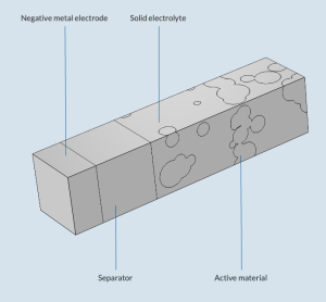 The geometry of the solid-state battery model.
Specialized physics interfaces and features make the setup of the model straightforward. The conservation of charge, mass, and momentum can be modeled with the Lithium-Ion Battery, Transport in Solids, and Solid Mechanics interfaces, respectively. There are also specialized features for modeling:
- Plating at the negative electrode
- Growth and shrinkage of the positive electrode
- Redox reaction at the electrode–solid electrolyte interfaces
 The SSB model and physics settings in COMSOL Multiphysics.
The simulation of the heterogeneous SSB evaluates certain quantities at the end of charge, including the electric and ionic potentials and von Mises stress in the solid electrolyte.
The results also include the evaluation of global quantities, including the cell voltage, state of charge, and stress in the z direction of the battery.
Paving the Way for SSBs
Looking into the mechanics of solid-state batteries with simulation can help researchers, automakers, and electronics companies incorporate SSBs into components and devices in the coming years — not decades.
The post Revamping a Solid-State Battery Cell appeared first on ELE Times.
The Rise of Smart Audio: From Sound to Intelligence
Courtesy: Infineon
What if your fridge warned you before it broke? Well, now it’s possible.
Imagine if your refrigerator hears a subtle vibration, predicting failure before it happens. Your oven guides you by the sound of your food sizzling. A health patch silently monitors your breathing patterns, alerting you to irregularities in real-time.
This is not science fiction. This is the sign of a new era, where audio drives intuitive, human-centric interactions between people and devices.
Audio as the interface: Beyond buttons and screens
Voice is the most natural interface we have ever known. Unlike traditional inputs, speech allows us to interact hands-free and eyes-free. This makes the technology ideal for daily tasks like cooking, driving, or assisting those with disabilities.
But to make this seamless and personal, technology needs more than a microphone. The solution demands:
- Persistent and ultra-efficient audio processing
- Robust AI, engineered to work together at the edge
Power and Performance — The Technology Behind Always-On Audio
Always-on audio relies on ultra-low-power architectures designed to listen continuously without draining energy. Modern microcontroller platforms now integrate autonomous analog subsystems capable of monitoring and pre-processing sound while operating in deep-sleep modes, enabling persistent listening with minimal power consumption.
Arm Cortex-M55
At the processing core, the Arm Cortex-M55 with Helium DSP extensions delivers significantly higher performance for embedded audio tasks—providing up to three times the efficiency needed for real-time signal processing, noise suppression, and on-device inference.
Neural Network Acceleration
Dedicated neural network accelerators further enhance these systems by offloading compute-intensive functions such as wake-word detection and voice activity recognition. This makes continuous listening feasible even in compact, battery-powered devices—from wearables to distributed IoT sensors—while maintaining fast response times and efficient power usage.
Intelligence – Software brings audio to life
DEEPCRAFT AI Suite is the engine behind transformative audio experiences. DEEPCRAFT Voice Assistant solution brings the following features, optimized for low-power Infineon MCUs:
- Accurate voice commands
- Custom wake words
- Keyword recognition
Speech-to-intent AI offers best-in-class performance with high accuracy and minimal false detects, while supporting both native and non-native English speakers.
DEEPCRAFT Audio Enhancement cleans up noisy environments with robust AI techniques:
- Noise suppression
- Acoustic echo cancellation
- Dynamic beamforming
These features are calibrated with easy-to-use tools for rapid integration. Developers can build, test, and deploy voice models via a no-code graphical UI, ensuring faster product development.
Integrated innovation – Affordability meets sophistication
Where once only expensive devices could offer clarity and smart voice recognition, PSOC Edge brings advanced edge audio to everyone.
Its built-in DSP capabilities and audio front-end middleware mean complex processing. From multi-mic beamforming to acoustic event detection, all happens within a single, efficient platform.
Furthermore, DEEPCRAFT’s AI-driven enhancements extend these advantages to cost-sensitive products like entry-level earbuds or low-cost smart sensors. This ensures everyone gets premium experiences.
Your next device, powered by Infineon audio innovation
With traditional solutions, advanced features like real-time voice and sound recognition have required expensive hardware or deep dependence on cloud-based computing. This limitation made them inaccessible to lower-end devices.
The synergy of PSOC Edge hardware and DEEPCRAFT software enables even resource-constrained devices to truly hear, understand, and act—all in real time, on ultra-low power, and with human-like intuition.
This breakthrough makes previously exclusive, cloud-dependent features available across a broader range of devices, democratizing intelligent functionality. Infineon is committed to building interfaces that empower people through natural, voice-driven interaction.
Takeaway
From predictive maintenance to voice-guided cooking, smart audio is reshaping how we live. Infineon’s integrated hardware and software make this transformation accessible to all, enabling high-quality, always-on audio experiences.
The post The Rise of Smart Audio: From Sound to Intelligence appeared first on ELE Times.
Serrated Edges: For Less Noise and Improved Fan Performance
Courtesy: Cadence
Understanding Noise Reduction in Industrial Fans
Industrial fans are widely utilized across various sectors, including manufacturing, automotive, and energy production, playing a vital role in ventilation and cooling. However, a notable drawback of these powerful machines is the significant noise they produce, which can range from 70 to 120 decibels. A primary contributor to this noise is the aerodynamic turbulence created by the fan blades. Addressing the challenges posed by the noise generated by industrial fans is a continuing focus of research in this area.
One promising avenue for reducing this noise involves passive noise mitigation methods, such as modifying the trailing edges of the fan blades. By incorporating designs with features such as sawtooth or serrated edges, we can effectively reduce noise levels without compromising performance. Computational fluid dynamics (CFD) studies of industrial fan designs can help pinpoint the optimal configuration that enhances performance and minimizes operational noise.
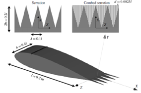 Sawtooth and combed-sawtooth trailing-edge serrations (Avallone et al., 2018)
In the webinar on CFD for Turbomachinery: Boost Performance & Control Noise, Antonis Karasavvidis, principal customer service engineer, and Domenico Mendicino, senior product engineering manager, examine a case study on the CFD analysis of industrial fan blades with serrated edges to understand how these modifications can effectively reduce the noise and enhance performance. This blog provides an overview of the case study presented in the webinar.
Overview: CFD Simulation of Industrial Fan with Serrated Edges
This case study examines the aerodynamic and acoustic performance of a ventilation fan, focusing on modifications to the blade design and their impact on airflow and noise characteristics under turbulent flow conditions. Starting with a baseline design, a ventilation fan was initially created using mean line design tools, achieving a blade tip Mach number of about 0.2. The design features a bell mouth at the inlet and blades constructed in three sections, utilizing NACA 65 profiles. This foundational design serves as a benchmark for subsequent modifications and performance evaluations.
Blade Variations and Design Enhancements
The study examines two types of serrated trailing edges added to the baseline design to achieve noise reduction and potential performance enhancements. These include:
- Variable Serration: A serration pattern applied with varying geometry along the blade’s trailing edge
- Uniform Serration: A consistent pattern cut along the trailing edge
Further enhancements include mechanical features such as embossing, pivots, and fillets, which are standard in this type of turbomachinery. Assessing these blade variations allows for comprehensive insight into their aerodynamic and acoustic effects.
Mesh Generation Workflow for Accurate Simulation
In this case study, Fidelity AutoGrid generates a high-quality, low-Reynolds-number mesh comprising approximately 2 million cells in approximately 20 seconds for the baseline design. This mesh is a structured multi-block grid with matching nodes on the periodic boundaries.
Given the complex geometries associated with the serrated trailing edges, an advanced mesh generation workflow was implemented, utilizing an unstructured mesh to capture the complex blade geometry while keeping the high-quality structured multi-block grid for most of the flow path. Utilizing Fidelity AutoGrid and ANSA, structured and unstructured grid strategies were combined to capture the intricate details efficiently.
Results of CFD Simulations
Using the GPU-enabled Fidelity Flow Solver, the simulations investigated the aerodynamic performance of the baseline design, uniform, and variable serrated blades. The solver provided rapid convergence within 200 iterations for the steady-state simulation and 3,600 time steps for an unsteady run with 10 inner iterations. Leveraging GPU acceleration on the Cadence Millennium platform provided high-fidelity results within minutes, even for the mixed-grid simulations.
The results indicated:
- Trailing Edge Effects: Serrations alter the pressure field near the trailing edges, particularly influencing the mixed-out flow downstream and the wake width
- Geometric Influence: Longer serration teeth facilitated enhanced energy exchange, correlating with improved aerodynamic performance
Additionally, the hub’s pivot and other mechanical features induced secondary flows, disrupting velocity profiles at the outlet and creating vortices, especially in the serrated configurations.
 Turbulent viscosity ratio distribution downstream of the blade for the baseline and uniform serration design
Noise Prediction and Analysis
The study evaluated noise characteristics through pressure fluctuations downstream of the trailing edge using both stationary and moving probes at different span heights. Key findings include:
- Stationary Probes: Minor differences in noise levels at various heights, dominated by blade-passing frequencies
- Moving Probes: Significant noise reduction effects at higher spans with serrated blades, while lower spans were governed by turbulence from the pivot and other design complexities
 Pressure fluctuations from the three probes located at span heights of 25%, 50%, and 75% on three different designs.
This case study highlights the aerodynamic and acoustic advantages of serrated trailing edges in ventilation fan design. By leveraging advanced mesh generation and GPU-based CFD solvers, the study achieved efficient simulations and precise results. The findings emphasize the importance of optimizing serrated geometries and conducting far-field noise analyses to refine fan performance, reduce noise emissions, and enhance design efficiency.
The post Serrated Edges: For Less Noise and Improved Fan Performance appeared first on ELE Times.
AI-Powered Semiconductor Design for EV Reliability: Why India Can Lead the Next Electronics Revolution?
By Sukhendu Deb Roy, Industry Consultant
Why India is uniquely positioned to lead the next electronics revolution by closing the loop between silicon, software, and the road?
Intro: India’s EV Electronics MomentIndia is at a powerful inflection point: a fast-growing EV market, a strengthening semiconductor design ecosystem, and a deep pool of AI and software talent. The real value in this transition will not come from assembling more electric vehicles alone, but from mastering the chips, power electronics, and intelligence that make EVs reliable, safe, and always available.

From SiC traction inverters to battery management systems (BMS) and telematics ECUs, EV reliability is fundamentally an electronics problem that plays out under harsh, real-world Indian conditions. For OEMs and their Tier-1 and Tier-2 partners, this shift means semiconductor decisions, electronics architecture, and AI strategy are no longer separate silos; together they determine uptime, warranty risk, and customer trust.
AI can close the loop between semiconductor device behavior and field performance, turning today’s reactive maintenance into tomorrow’s predictive and self-healing EV ecosystems.
Takeaway: AI-powered semiconductor and EV electronics design can shift reliability from reactive repairs to predictive and self-healing systems, cutting failures, downtime, and warranty costs by roughly 40–60% over time — and India is uniquely placed to lead this shift.

Every EV reliability story starts at the device level. Choices around Si/SiC MOSFET design, IGBT technology, gate-driver strategies, packaging, and thermal paths determine switching losses, heat, and long-term stress in traction inverters and onboard chargers. Under Indian duty cycles
— high ambient temperatures, stop-go traffic, overloaded vehicles, and poor roads — those design decisions show up later as derating, efficiency loss, or outright failures.
The same applies to battery cells and BMS hardware: cell chemistry, form factor, and sensing strategies determine how accurately the system can “see” degradation or thermal risk. When this visibility is poor, fleets experience unexpected range drops, thermal events, and a costly pattern of warranty claims and field fixes.

Traditional semiconductor and power-electronics design relies on simulations, design for reliability (DfR), lab validation, and field-return analysis. AI adds a new, continuous feedback loop: it learns from billions of switching events, thermal cycles, and usage profiles observed in real vehicles, and feeds that learning back into both device design and control algorithms.
This loop uses signals such as high-frequency waveforms, temperature gradients across modules, vibration signatures, and battery state-of-health (SoH) curves to identify stress patterns and precursors to failure. Over time, designers can co-optimize silicon, packaging, and firmware for actual Indian operating conditions rather than idealized lab scenarios — improving both first-time-right silicon and long-term field reliability.
A quick India scenario: Imagine a 2-wheeler fleet in Chennai. AI models trained on inverter waveforms and temperature data across thousands of rides can flag an emerging failure pattern in a particular batch of power modules and trigger an OTA-driven derating and firmware fix before riders see breakdowns.
Four AI Capabilities That Change EV Reliability Predictive BMS Intelligence (Cell-level)Batteries are the single largest cost item in EVs and one of the most reliability-critical. AI models can continuously learn from cell voltages, temperatures, internal resistance evolution, and charge–discharge histories to detect early degradation, thermal runaway risk, and balancing drift at cell level. For Indian conditions — high temperatures, frequent partial charging, and stop-start usage — such predictive BMS intelligence can extend usable battery life by double-digit percentages and materially improve safety. Better SoH and range estimation also reduce range anxiety for drivers and allow fleet operators to plan maintenance proactively.
Traction inverters and motors sit at the heart of EV performance, directly built on semiconductor device and magnetic design Machine-learning models can analyse switching waveforms, current and voltage harmonics, torque–speed behavior, vibration patterns, and thermal maps to catch subtle anomalies long before a fault triggers a visible error. This enables early detection of gate-drive misbehavior, partial shorts, insulation degradation, bearing wear, and cooling issues that would otherwise surface as roadside failures or derated power. At fleet scale, such diagnostics can realistically cut unexpected drivetrain failures by 30–50%, significantly improving asset utilization.

Diagnostics alone are not enough; systems need a way to act on insights in the field. Over-the-air (OTA) firmware platforms, combined with AI, can detect abnormal behavior in ECUs, roll back to known-good images, patch vulnerabilities, and adjust control parameters to protect power devices and batteries. For example, if analytics indicate elevated stress on a particular inverter design in hot regions, OTA updates can modify switching patterns, current limits, or thermal thresholds to reduce risk without requiring a workshop visit. OEMs already see significant warranty and recall savings from OTA-based fixes; AI-guided self-healing will deepen this advantage and improve customer experience.

The full power of AI emerges when every vehicle becomes a data node. Connected EVs stream anonymized health, usage, and environment data to the cloud, where AI aggregates patterns across cities, duty cycles, and seasons. Refined diagnostic and control models are then pushed back to vehicles via OTA, closing the loop from chip to cloud and back.
In this paradigm, EVs do not just age; they improve over time. Updated BMS models provide better SoH estimates, inverter control becomes more efficient, and fault detection grows more sensitive with every kilometer driven. The same hardware platform becomes more valuable with each software and model refresh — a powerful shift in how the industry thinks about lifecycle value.

Evidence from other industries shows that AI-driven predictive maintenance can reduce unplanned downtime by about 30–50% and cut maintenance costs by 18–25% through earlier fault detection and better planning. At the same time, connected diagnostics and OTA capabilities allow OEMs to resolve many issues remotely, significantly lowering warranty and recall costs.
When these approaches are applied systematically across EV batteries, powertrain electronics, and software — and when semiconductor and system design are instrumented for rich telemetry — it is credible to target 40–60% improvements in reliability metrics and warranty economics over a multi-year horizon. This magnitude of impact justifies serious investment from OEMs, Tier-1s, Tier-2s, and policymakers.

- OEMs
- Define EV reliability KPIs (uptime, failure rates, cost per vehicle) that explicitly depend on electronics and AI, not just mechanical systems.
- Mandate data pipelines, OTA capabilities, and diagnostic hooks as core requirements in platform and supplier specifications.
- Tier-1 suppliers (inverters, BMS, ECUs, telematics)
- Design hardware and firmware with AI-grade observability: rich sensing, timestamped logs, and secure connectivity interfaces.
- Offer OEMs diagnostics and predictive-maintenance APIs as part of the product, not as optional add-ons.
- Tier-2 and component suppliers (devices, sensors, boards)
- Expose relevant device-level health signals (e.g., temperature, switching counters, error events) that higher-level ECUs and cloud models can consume.
- Collaborate with Tier-1s on test data, stress conditions, and failure signatures to make AI models more accurate.

India is already emerging as a major center for semiconductor design, verification, and R&D services, with global chip majors expanding their engineering presence in the country. Parallelly, the domestic EV market — particularly in 2-wheelers, 3-wheelers, and commercial fleets — is scaling rapidly, creating demanding real-world use cases that generate rich data for AI models.
This combination positions India to move beyond low-cost manufacturing and become a global hub for EV electronics intelligence, including:
- AI-optimized power device reference designs for SiC/IGBT
- Predictive and interpretable BMS/Inverter control
- Validated OTA/diagnostics platforms for fleet
These are exportable IP and platform plays that can serve global OEMs, not just domestic brands, while also anchoring higher-value electronics manufacturing within India.

To capture this opportunity, India’s ecosystem needs alignment across six pillars:
- Semiconductor & power-device design: Build AI-ready telemetry and reliability sensing into devices and modules from the outset.
- Power-electronics & system integration: Architect inverters, BMS, and ECUs for rich observability and secure connectivity.
- Software-defined vehicle architectures: Treat data collection, model deployment, and OTA as first-class design goals, not afterthoughts.
- Secure-by-design engineering: Ensure that telematics, OTA, and data flows are robust against cyber threats.
- Validation & standards: Extend traditional validation with AI-driven test generation, digital twins, and continuous in-field learning loops.
- Interdisciplinary Talent Development: Fund research and training programs to explicitly create hybrid talent (e.g., AI engineers specializing in power electronics and thermal physics) required to bridge the gap between device design and fleet data.
If OEMs, Tier-1s, Tier-2s, chip companies, startups, and policymakers work together across these pillars, India can define the template for AI-powered semiconductor design and EV reliability — and, in doing so, help lead the next global electronics revolution.

Email: mailsukhendu@gmail.com
LinkedIn: Sukhendu Deb Roy
The post AI-Powered Semiconductor Design for EV Reliability: Why India Can Lead the Next Electronics Revolution? appeared first on ELE Times.
Kyocera and Rohde & Schwarz’s multipurpose phased array antenna module (PAAM) at CES 2026
Kyocera and Rohde & Schwarz will demonstrate the characterization of Kyocera’s novel phased array antenna module (PAAM) at CES 2026 in Las Vegas, NV. The demonstration at the Kyocera booth will feature the R&S ATS1800M 5G NR multi-directional mmWave test chamber from Rohde & Schwarz, known for its exceptionally small footprint and over-the-air (OTA) testing capabilities.
Kyocera has developed a novel phased array antenna module (PAAM) for a variety of sensing and communications applications. Featuring 384 dual-polarization elements, the PAAM can create up to eight simultaneous beams with varying directions and frequencies. This design incorporates 6G ISAC (Integrated Sensing and Communication) technology that combines wireless communication and sensing into a single framework. It allows networks to simultaneously deliver data and sense their environment, unlocking applications such as next-generation autonomous driving, environmental sensing, and industrial automation – all with greater efficiency and performance.
Ensuring all antenna elements work cohesively to form an RF beam with the desired characteristics is critical. Rohde & Schwarz offers a patented over-the-air (OTA) testing approach within a fully shielded environment, allowing engineers to verify beam patterns and minimize sidelobes.
The R&S ATS1800M is a unique solution featuring four feed antennas and CATR reflectors, each providing a 30 cm quiet zone (QZ). At CES 2026, the Kyocera PAAM device under test (DUT) will be positioned on a rugged 3D positioner at the center of the four overlapping QZs. This configuration allows Kyocera’s engineers to conduct a variety of tests, including the simultaneous reception of RF beams from multiple directions. The patented vertical CATR design minimizes the system’s lab footprint compared to other OTA solutions.
The complete test setup incorporates multiple instruments from Rohde & Schwarz, including signal generators and analyzers alongside the mmWave test chamber, providing a fully integrated testing environment. The device under test receives four independent signals via the chamber’s reflectors, simulating complex reception scenarios, and the resulting signal quality is measured and analyzed. This comprehensive system enables thorough evaluation of the phased array antenna module’s performance in realistic conditions.
Visitors to CES 2026 can experience this milestone demonstration live at the Kyocera booth (6501) in the West Hall of the Las Vegas Convention Center, from January 6 to 9, 2026.
The post Kyocera and Rohde & Schwarz’s multipurpose phased array antenna module (PAAM) at CES 2026 appeared first on ELE Times.
AI PCs: What Tata Electronics and Intel Aim to Scale in India
Tata Electronics, a global enterprise headquartered in India, and Intel Corporation, a US-based manufacturer of advanced semiconductors, have announced a strategic alliance to explore manufacturing and packaging of Intel products for the Indian Market at Tata’s upcoming Fab and OSAT plants. As part of the same MoU, the partnership between the companies also intends to scale up tailored AI PC solutions for consumer and enterprise markets in India. The AI PC market is expected to be one of the Global top 5 markets by 2030.
But what exactly is an AI PC?
An AI PC is a computer with a dedicated Neural Processing Unit (NPU) that renders unflinching reliability and speed to the AI processes over a PC. Such PCs can run large AI models locally as they are not heavily dependent on the cloud for functioning.
What is a Neural Processing Unit (NPU)?
A Neural Processing Unit (NPU) is a low-power yet dedicated chip installed only for AI/ML workloads. It consumes 10-20 percent less power as compared to conventional GPUs. It can efficiently handle everything from real-time language translation and speech-to-text to advanced vision tasks, and even the functions of a personal AI assistant.
Enhanced Security & Privacy
In Such PCs, local NPU-based AI execution ensures that private data remains on the system, minimizing cloud dependency and elevating overall security and confidentiality. It also excels in managing system resources intelligently for better performance and battery life.
Intel-Tata Collaboration
This collaboration would leverage Intel’s AI compute reference designs, Tata Electronics’ industry-leading Electronics Manufacturing Services (EMS) capabilities, and broad access to the Indian market through Tata Group companies. This collaboration marks a pivotal step towards developing an India-based geo-resilient electronics and semiconductor supply chain.
N Chandrasekaran, Chairman, Tata Sons, said, “The Tata Group is deeply committed to developing a robust semiconductor industry in India. We are excited to collaborate with Intel, and this strategic alliance would accelerate our efforts. Together, we will drive an expanded technology ecosystem and deliver leading semiconductors and systems solutions, positioning us well to capture the large and growing AI opportunity.”
The post AI PCs: What Tata Electronics and Intel Aim to Scale in India appeared first on ELE Times.
UP’s Semiconductor Push: State to Build Three New Electronics Hubs Beyond NCR
With an aim to boost development and employment beyond the traditional Noida-Greater Noida belt, the UP government is planning to set up three semiconductor hubs in the hinterland. The set up is expected to be established in Pilibhit, Barabanki, and Gorakhpur.
Government has strategically chosen these locations to tap local resources and improve connectivity in the region while reducing the pressure of over-urbanization in the western industrial region of the state. These three facilities will be part of the Electronics System Design and Manufacturing (ESDM) Initiative. The facilities are expected to attract private investment, generate skilled employment, and create a more balanced industrial demographic across the underdeveloped districts in the state.
Through this policy, Uttar Pradesh aims to become the prime state to fulfil the country’s electronic needs. It is already a key contributor of mobile manufacturing and other electronic components through facilities established in Noida and Greater Noida.
Anurag Yadav, Principal Secretary (IT and Electronics), said that UP is strengthening its position in the high-value electronics sector and attracting companies to set up operations. He confirmed that four anchor firms have already begun establishing their facilities.
The post UP’s Semiconductor Push: State to Build Three New Electronics Hubs Beyond NCR appeared first on ELE Times.
Pages

