
Новини світу мікро- та наноелектроніки
Freehand Pcb creation with 555 flasher.
 | I want to make my own PCBs, but i find all the PCB design programs infuriating. So i have been honing my free hand skills, using blank copper clad board and an etch resistant pen. This, a simple 555 flasher, is my latest one. I used a SOIC 555 with 0805, and 0603 surface mount supporting components. [link] [comments] |
Generative Artificial Intelligence Boosts Chip Yields and Slashes Manufacturing Defects
In 2021, car manufacturers worldwide halted production because a single one-dollar microcontroller was unavailable. The wait time for advanced semiconductors jumped from 12 weeks to over 26 weeks, revealing how fragile the global supply chain had become. The yield losses and manufacturing defects are not just technical issues-they are strategic challenges affecting procurement leaders, supply chain managers, and even national economies.
Meanwhile, demand for semiconductors continues to grow relentlessly. Global consumption is expected to increase at a compound annual growth rate of 7 to 8 percent through 2030, while production capacity is only growing at about 5 percent per year. This mismatch makes every wafer incredibly valuable. Even a modest 2 percent improvement in yields at advanced technology nodes could free up around 150,000 wafers annually, which translates into billions of dollars of extra supply.
Generative AI addresses these challenges by creating optimized designs in advance, anticipating potential defects, and enhancing scheduling in wafer fabrication. It is reshaping the economics of the semiconductor industry- improving yields, reducing inconsistencies, and strengthening supply chains’ reliability.
The Yield Challenge in Semiconductor Manufacturing
Chip manufacturing involves more than 1,000 steps, from photolithography to etching. At advanced nodes of three nanometres and below, tiny atomic-level variations can make wafers unusable. With single-wafer costing over 16,000 dollars, any loss in yield directly cuts profit margins.
Every percentage point of yield improvement is like adding a new fabrication plant without capital investment, said Sanjay Mehrotra, CEO of Micron Technology.
How Generative AI Creates Strategic Value
Generative models such as Generative Adversarial Networks (GANs), Variational Autoencoders (VAEs), and foundation models go beyond predictive analytics: they generate better alternatives. Four applications stand out:
- Design Optimization
Generative AI evaluates thousands of layout variations to identify configurations that reduce defects. Synopsys, working with Taiwan Semiconductor Manufacturing Company (TSMC), reported a 15 percent yield improvement using AI-driven design space exploration. Faster design cycles and quicker delivery to customers follow. A European fabless design company leveraged generative AI for design optimisation and achieved ROI in just 18 months, reducing wafer scrap, accelerating revenue realization, and lowering operational costs.
- Defect Prediction
AI generates synthetic wafer maps to train inspection systems before defects appear. American-based KLA corporation reported 25–30 percent improvement in defect detection, resulting in more usable wafers and faster production cycles. Samsung implemented AI-based yield learning to cut line failure rates by 12 percent, decreasing buffer inventory needs and improving delivery reliability.
- Assistance with Lithography
AI supports mask patterns generation to minimize distortions through Inverse Lithography Technology (ILT) and Optical Proximity Correction (OPC). Intel reported a 40 percent reduction in edge-placement error, increasing first-pass yields.
- Supply Assurance and Fabric Scheduling
Generative AI simulates thousands of scheduling scenarios, balancing tool usage, and maximizes throughput. A Taiwanese fabless company reduced wafer cycle times from 20 to 17 days using AI scheduling, ensuring timely chip delivery in a competitive market.
It also strengthened broader supply chain resilience. Global Foundries applied predictive analytics to reduce recovery times during material shortages by 30 percent, helping procurement meet client demand during disruptions.
Industry Case Studies and Outcomes
- Samsung Foundry – AI-based Yield Learning- It reduced the cut line failure rates by 12 percent, lowering buffer inventory requirements and improving delivery reliability for customers.
- Global Foundries – Predictive Supply Chain Analytics: Using predictive analytics, it improves supply chain resilience and cuts recovery times during material shortages by 3 percent, enabling procurement teams to meet client demands.
- European Fabless Design Company – Design Optimisation: Employing generative AI for layout optimisation, the company achieved return on investment (ROI) in just 18 months. By decreasing wafer scrap, speeding revenue realisation, and reducing operational cost.
Strategic Procurement and Supply Chain Value
Generative AI serves the dual role. On the shop floor, it functions like examining billions of flaw patterns to increase yields. In the boardroom, it mitigates risk, strengthens supply continuity, and protects margin.
Predictive insight facilities by generative AI can help with lead time optimisation, multi-sourcing strategy guidance, and supplier negotiations, and align contractual requirements with actual fab performance, ensuring reliable capacity guarantees.
SEMI CEO Ajit Manocha stated that generative AI is not just yield enhancement-, it lowers process variability, increases predictability, and strengthens overall operational resilience.
Challenges to Adoption
Despite its transformative potential, adopting generative AI in the semiconductor industry presents several challenges:
Ø Data confidentiality: It remains the key concern because the processed data is so proprietary and difficult to share across ecosystems.
Ø Computational intensity: It requires a substantial amount of computational equipment to train sophisticated AI generative models.
Ø Explainability gaps: To foster confidence, engineers and procurement teams need AI advice to be transparent.
Ø Change management: To fully realise value, Fabs must retrain process engineers, educate procurement specialists in AI literacy, and link data science teams across silos.
The Road Ahead: Toward Autonomous and Resilient Fabs
Next-generation semiconductor factories are increasingly relying on generative AI as central intelligence. Emerging trends include:
- Autonomous fabs: It leverages generative AI to modify recipes in real time to reduce yield loss and improve efficiency.
- Collaborative ecosystems: Design firms, equipment manufacturers, and fabs share AI models to optimize production and supply chain resilience.
- Zero-defect manufacturing: While idealistic, generative AI is making substantial progress towards achieving it, bringing fabs closer to near-perfect yield and consistency.
Strategic Imperatives for Leaders
The path forward is clear for procurement executives, semiconductor leaders, and strategy decision makers:
- Scale AI across operations: Transition from pilots to full integration in scheduling, lithography, electronic design automation, and inspection workflow.
- Leverage AI in procurement: Use insights for contract negotiations, supplier diversification, and lead time predictability.
- Invest in people and collaborations: Integrate the expertise of supply chain managers, data scientists, and strengthen collaboration with AI solution providers and academic institutions.
Conclusion
Generative AI is transforming chip manufacturing. It boosts yields, cuts defects, and improves production scheduling. More importantly, it helps leaders make supply chains stronger, margins steadier, and delivery times more predictable.
Companies that embrace AI first will unlock extra capacity, protect supply continuity, and gain a clear competitive edge. Every wafer counts, and every week of lead time matters. Generative AI ensures neither is wasted.
The post Generative Artificial Intelligence Boosts Chip Yields and Slashes Manufacturing Defects appeared first on ELE Times.
NREL’s silicon carbide-based ULIS power module claims record efficiency, power density, and low-cost manufacturability
Apple’s 2H 2025 announcements: Tariff-touched but not bound, at least for this round

On Tuesday, Apple, as usual for a September, unveiled its latest-generation tranche of iPhones, Apple Watches, wireless headphones, and the like, at its as-usual-prerecorded “Awe Inspiring” event (here’s last year’s event coverage from yours truly, if a preparatory memory refresh is necessary). Admittedly, there wasn’t anything terribly surprising unveiled, in no small part because much of it was predictable (last year’s iPhone 16 series was superseded by this year’s 17 series, for example…duh…) and a lot of it was also inevitable, “thanks” to the usual internal, partner (case suppliers and cellular carriers, for example) and supply chain players’ in-advance leaks. Never fear, however: I still found plenty of interesting (at least to me) tidbits big-and-small that I’ll be sharing in the following sections.
The chipsI’ll start with what the engineers out there are most interested in: the new phones’ internals. Much as the generational number-naming cadence for the new phones (three of them, at least: hold that thought) was predictable, so too is the cadence for their SoCs: last year’s A18 processors have been superseded by A19s (again…duh). And as usual, we don’t have a lot of details on them—clock speeds, cache size specifics, etc.—although Geekbench benchmarks on the “Pro” variant are already published. So, what do we know? Here’s the baseline A19, with a CPU cluster comprised of two performance and four efficiency cores, and a five-core GPU:


And here’s what Apple says about it:
Built on third-generation 3-nanometer technology, A19 delivers powerful performance, efficiency, and a huge boost in speed. An updated display engine, ISP, and Apple Neural Engine power features like Apple Intelligence and the latest-generation Photographic Styles. The 6-core CPU is 1.5x faster than the A15 Bionic chip in iPhone 13, and the 5-core GPU is more than 2x faster than A15 Bionic, unlocking stunning graphics and next-level mobile gaming. Neural Accelerators are also built into each GPU core to help run powerful generative AI models on device.
 For comparison’s sake, the A18 was also a two-performance-core/four-efficiency-core CPU cluster architecture, with GPU core counts from four to six depending on the target device, albeit “binned” during test from the exact same originating sliver of silicon, I ‘spect.
Now for the A19 Pro:
 Same two-performance-core/four-efficiency-core CPU cluster architecture as the baseline A19. So, what’s the “diff”? Apple claims that the “Pro” performance cores have both enhanced branch prediction and front-end bandwidth, and the new efficiency cores have more “last-level” (likely translation: core-shared) cache: a 50% capacity boost, to be precise. Now for the GPU:


Two graphics cluster options, at least so far: 5- and 6-core counts. Stay tuned for which phone(s) each goes into. And here’s what Apple says about the A19 Pro:
A19 Pro is Apple’s most capable iPhone chip yet. When paired with the Apple-designed vapor chamber, A19 Pro enables iPhone 17 Pro and iPhone 17 Pro Max to deliver up to 40 percent better sustained performance than the previous generation — ideal for gaming, video editing, and running large local language models. The 6-core CPU is the fastest CPU in any smartphone, and the 6-core GPU architecture includes Neural Accelerators built into each GPU core, a larger cache, and more memory than A18 Pro. The GPU works in tandem with the new 16-core Neural Engine to power Al models, stunning graphics, and AAA gaming titles like Arknights: Endfield, enabling hardware-accelerated ray tracing and higher frame rates.
Following both Apple-authored paragraphs I’ve already shared is another one, revealing another IC, this one more revolutionary versus evolutionary, although the concept’s already proven:
The iPhone 17 lineup also introduces N1, a new Apple-designed wireless networking chip that enables Wi-Fi 7, Bluetooth 6, and Thread. In addition to powering the latest generation of wireless technologies, N1 improves the overall performance and reliability of features like Personal Hotspot and AirDrop.

Apple has long stated its aspiration to “own” as much of the silicon foundation of its products as possible—with the likely exclusion of DRAM and flash memory, along with image sensors—although long-term on that last one, who knows? Broadcom had historically been Apple’s predominant supplier of wireless networking technology, although Apple had already ventured out on its own with earbuds (Bluetooth) and smart watches (both Bluetooth and Wi-Fi). That said, and perhaps obviously, the N1, whose development was rumored back in December, is a notable advancement on this foundation from both performance and functionality standpoints, including the welcome inclusion of Matter-related Thread support.
And speaking of wireless connectivity, what about the cellular side of the family? Apple’s iPhone 16e, introduced earlier this year, had first-time included the company’s in-house-developed cellular subsystem, the C1. Now there’s the C1X successor:
C1X, a new cellular modem designed by Apple…is up to 2x faster than C1, and for the same cellular technologies, it is even faster than the modem in iPhone 16 Pro, while using 30 percent less energy overall. This makes C1X the most power-efficient modem in an iPhone.

That said, the C1X is included in only one of this September’s new phones. Here’s a hint: power consumption is particularly critical with this particular mystery phone model. And the downside: as a result, it doesn’t support mmWave 5G cellular data services. Stay tuned for the details (assuming you haven’t already figured it out after visiting one of the earlier links).
One other IC-related advancement, supported by the A19 SoC series (and presumably future A-, M-, and other-series chips as well), bears mention. It’s Memory Integrity Reinforcement, which Apple describes as follows within a detailed Security Engineering and Architecture (SEAR) post:
Memory Integrity Enforcement (MIE) is the culmination of an unprecedented design and engineering effort, spanning half a decade, that combines the unique strengths of Apple silicon hardware with our advanced operating system security to provide industry-first, always-on memory safety protection across our devices — without compromising our best-in-class device performance. We believe Memory Integrity Enforcement represents the most significant upgrade to memory safety in the history of consumer operating systems…
Memory Integrity Enforcement is built on the robust foundation provided by our secure memory allocators, coupled with Enhanced Memory Tagging Extension (EMTE) in synchronous mode, and supported by extensive Tag Confidentiality Enforcement policies. MIE is built right into Apple hardware and software in all models of iPhone 17 and iPhone Air and offers unparalleled, always-on memory safety protection for our key attack surfaces including the kernel, while maintaining the power and performance that users expect.
With all due respect, SEAR might have gotten at least a bit out over its skis; conceptually similar schemes have already been implemented by Microsoft (in Windows 11) and Arm (supported, for example, by Google beginning with the Pixel 8 series). That said, as The Verge notes:
Apple says its implementation goes a step further, with the ability to protect all users by default and by designing its A19 and A19 Pro chips for enhanced security, while still adding memory safety changes for older hardware that doesn’t support the new memory tagging features. The company also says its new mitigation for Spectre V1 leaks works with “virtually zero CPU cost” — as performance hits have been an issue for memory integrity and other security features — with all of the changes making “mercenary spyware” even more expensive to develop.
Time will tell, I suppose.
The iPhone 17s (iPhone 17)

(iPhone 17 Pro Series)
Nearly 1,500 words in, and I haven’t even gotten to the products themselves yet? Oh, bother. Let’s speed things along for the remainder of this piece by switching to bullets where possible:
- There are three of them this time: the baseline iPhone 17, the high-end iPhone 17 Pro, and the Pro Max.
- The iPhone 17 runs the baseline A19 SoC, while both “Pro” models embed the six-GPU-core variant of the A19 Pro.
- iPhone 17 capacities start at 256 GBytes, for the same $799 price tag that the 128 GByte iPhone 16 sold for a year ago. That same 128 GByte iPhone 16, now selling for $100 less ($699), is the only capacity variant of that particular 16th-generation model still offered by Apple for purchase (along with both 128 GByte and 256 GByte versions of the iPhone 16 Plus, interestingly, as well as the more recently introduced iPhone 16e, of course). And of course, the iPhone 15s have been expunged from the company’s product line.
- Turn to the Pro variants, and things get even more interesting. Again, there’s no 128 GByte 17th-generation option. But no iPhone 16 Pros (or Pro Maxes, for that matter) are being sold any longer, either, so $1,099 (in fairness, matching what the 256 GByte iPhone 16 sold for a year ago) is now your lowest-priced 17 Pro entry point (therein explaining the “touched by tariffs” nuance in this post’s title). And hey, if you’ve got $2,000+ sitting around begging to be burned, you could instead spend it on a 2 TByte iPhone 17 Pro Max…
- I find this quite interesting; all three phones are sold in both physical SIM (only in some countries) and eSIM-only options. What did Apple do with the internal space freed up by the removal of the physical SIM tray and other hardware bits? They instead devoted it to higher-capacity batteries, at least for Pro models; eSIM-only phones spec longer between-charges operating life.
- In today’s example of “insincere feature set restrictions in order to encourage purchase upgrades”, the USB-C port on the iPhone 17 only runs at USB2-compatible 480 Mbps data transfer rate speeds. Should you wish to shoot video on one of them, you’ll quickly run out of internal storage and then realize that the tethered external-storage bandwidth isn’t up to snuff, either…or you could just proactively buy an iPhone Pro model instead. And before you point to the A19-vs-A19 Pro differentiation as the root cause…the other just-released iPhone (which I’ll discuss next) is A19 Pro-based, but is USB2-only, too.
- Speaking of video (and image capture more generally); both rear cameras on the iPhone 17 now have 48 Mpixel image sensors (vs 12 Mpixels for the ultrawide in the iPhone 16). The same goes for the three cameras on the Pro models (on the 16th generation predecessors, the telephoto was 12 Mpixels). And all three models’ front cameras not only bump up the resolution from 12 Mpixels to 16 Mpixels but also support Center Stage AI-enabled algorithms that dynamically crop and interpolate to keep subjects centered in the frame.
- The displays are now protected by next-generation Ceramic Shield 2 coatings; the back panel on Pro models now has prior-generation Ceramic Shield protection, too. As for sizes and such, the iPhone 17 makes the biggest jumps; from 6.1” diagonal to 6.3” (along with generationally shrunken bezels), now also supporting dynamically switching (to optimize for at-the-moment application need vs battery life, which Apple brands as ProMotion) refresh rates up to 120 Hz (and down to 1 Hz).
- The Pro devices’ frames are now once again aluminum-fabricated, fundamentally (presumably) to simplify the fabrication process and otherwise reduce cost (of the raw material, along with allowing for reuse of scrap) vs titanium. Tariffs strike again…
- And whereas the baseline iPhone 17 RAM capacity is generationally unchanged at 8 GBytes, the Pro variants bump it from 8 to 12 (reportedly) GBytes. AI strikes again…
- Oddly, there’s no black (or near-black) color option offered for either of the Pro models
- All three models continue to rely on Qualcomm cellular subsystems, presumably (if for no other reason) to afford them with optional mmWave 5G support.
- And last, but not least: does that new backside-spanning “camera bar” arrangement for the iPhone 17 Pro models remind you at least somewhat of a Google Pixel, or what?
![]()
Apple sells “Air” laptops. And “Air” iPads. So, you had to know an “Air”-monicker iPhone was going to arrive sooner or later, right? Right.

A quick aside, once again with the big-picture theme of tariff-counteracting moves to preserve profits. Keen-eyed readers might have noticed that there’s no 6.7″ “Plus” iPhone version in this generation. Granted, the baseline iPhone 17 display is a smidge bigger than it was before, as already noted. But want something brand-new and even bigger, and you’ll need to jump all the way up to the $1,199-or-higher 6.9” iPhone 17 Pro Max…or make a lateral move instead, to the $999-or-more 6.5” iPhone Air.
What do you get for paying $200 more than a baseline iPhone 17 of the same capacity?
- The aforementioned slightly larger display
- The aforementioned more powerful CPU (although this version of the A19 Pro is only “binned” for five active GPU cores, and I’m betting it’s also comparatively underclocked for thermal and battery life reasons)
- A 1 TByte capacity option (for “only” $1,399)
- 09 inches/2.16mm less thickness (0.34 inch/8.75 mm for the iPhone Air, versus 0.31 inch/7.80 mm for the iPhone 17)
- 42 ounces/12 grams less weight (5.82 ounces/165 grams for the iPhone Air, versus 6.24 ounces/177 grams for the iPhone 17)
- And a titanium-based frame. Apple apparently was loath to have another “Bendgate” on its hands…bad pun intended:
And what do you lose, beyond an extra $200? Well…
- A second backside camera
- mmWave 5G cellular data connectivity (this is the “mystery model” mentioned earlier, based on Apple’s C1X chip, if you hadn’t already figured it out)
- Battery life: a 3,149 mAh battery for the iPhone Air, not counting the $99 Air-only MagSafe external battery, versus 3,692 mAh for the iPhone 17
- Slower charging speeds: 20W-max MagSafe and USB-C charging on the iPhone Air, again presumably due to thermal concerns, versus 25W MagSafe and 40W (60W burst) USB-C charging on the iPhone 17
- A physical SIM option, at least in some countries (the iPhone Air is eSIM-only, to squeeze as much battery capacity inside as possible for operating life reasons, presumably)
- And no “17” generational qualifier
 (which makes me wonder just what the company will call the next one?)
But hey, just like the iPhone 17, the iPhone Air also supports only USB2 480 Mbps-max wired data transfer rates (as I hinted at earlier), so…sigh.
The Apple Watches
(Apple SE 3)

(Apple Series 11)

(Apple Watch Ultra 3)
Nearing 2,500 words. Oh, d-d-d-dear! Apple’s newest-generation watches are modest-at-best upticks from their precursors, truthfully. The SE 3 and Ultra 3 have migrated from the S9 to S10 SoC internally…that said, it’s long been rumored that Apple’s kept its smartwatch SoCs pretty-much-to-completely identical the past few generations, only altering the name stamped on top. Befitting this potential reality, the S10 stays the same from the Series 10 to the new Series 11.
All three watches gain new health-monitoring and -analysis capabilities, which Apple admittedly, surprisingly, also plans to retrofit to recent past smartwatch generations. The entry-level SE 3 also inherits the previous mainstream-and-above-only always-on display option. At the high end, the Ultra 3 gets direct-connect satellite communications capabilities…nearly three weeks later than the notably more affordable (roughly half the price, in fact) Google Pixel Watch 4, and nearly a week behind Garmin’s also-satellite-cognizant fēnix 8 Pro. Oh, and dual-band GPS. See earlier versus-Google Pixel Watch 4 comment.
The AirPods Pro 3
Last, but not least, new-generation high-end Bluetooth earbuds (following their year-ago updated mainstream siblings). Y’know, when references to an unannounced product show up in released (albeit beta) software, my general rule of thumb is that the product won’t stay unannounced for long, capisce?
Here’s what Apple claims about the AirPods Pro 3:
AirPods Pro 3 deliver unbelievable sound quality and the world’s best in-ear Active Noise Cancellation (ANC) — removing up to 2x more noise than the previous-generation AirPods Pro, and 4x more than the original AirPods Pro.
Independent rumors and ears-on analysis admittedly back up the company’s comparative-ANC claims, but are more reserved in their audio-quality improvement assessments (then again, when I want to do critical music listening, Apple earbuds are not what I’d think to grab first…or second…or…). The H3 SoC upgrade-enabled inclusion of heart-rate detection is interesting; I just hope that lightning doesn’t strike twice, re Apple-owned Beats’ Powerbeats 2 inability to walk and chew gum at the same time (more accurately: play music while tracking heart rate on gym equipment). I mean…isn’t listening to music the fundamental point of these things?
Live language translation (and live broadcast of that translation to another AirPods set wearer) is something I very much look forward to trying out..and I will, because ever-generous Apple is backfilling the feature to the AirPods Pro 2, too (Q: Did you say AirPods Pro 2, Brian? A: Yes, I did, and genuine ones too; a story for another day). The transition from silicon to foam ear tips is interesting, too. And generally-generous Apple now includes five different-sized tip sets for optimal user fit purposes. But generosity has limits. No bundled USB-C cable (any more) for you. Have I yet mentioned tariff costs leading to counterbalancing cost reductions elsewhere?
MiscellanySpeaking of wireless earbuds, shortly before the launch event, a teaser video of Beats’ latest Powerbeats Fit appeared on Apple’s own YouTube channel:
But as I write these words, they’re not yet officially announced. My theory: Apple intentionally held them back, wanting to showcase earbuds that only work with Apple devices versus (also? Instead?) introducing ones that were cross-platform, including…insert ominous pipe organ sound…Android.
Other tidbits:
- Much as I’ve needled Apple versus Google in this writeup, I’m compelled to point out that all the products that Apple announced on Tuesday will be available for preorder on Friday, September 12, with in-store sales (and shipments) commencing the following Friday, September 19. In contrast, a notable chunk of what Google announced three weeks ago won’t be available until next month.
- Speaking of dates, the various “26” operating systems unveiled at WWDC in June will all “go gold” on Monday, September 15. That said, I’ve already got the “gold” versions of Google’s Material 3 Expressive revamps running on my Pixel phones and Pixel Watch and am lovin’ em, so….

- And one final bit of evidence of Apple’s (sometimes) generosity: the company has extended its free satellite connectivity promotion to iPhone owners for another year.
So, there you go: an as-usual mix of the impressive, the mundane, and multiple points in between. That said, who am I trying to fool? “It’s all for naught;” Apple will sell everything it’s got (yes, especially the iPhone Air). Having passed through 3,000 words a few paragraphs ago, undoubtedly spiking poor Aalyia’s blood pressure in the process, thus concludes today’s Winnie the Pooh-themed post. Let me know your thoughts in the comments!
—Brian Dipert is the Editor-in-Chief of the Edge AI and Vision Alliance, and a Senior Analyst at BDTI and Editor-in-Chief of InsideDSP, the company’s online newsletter.
Related Content
- It’s September in Apple land, so guess what it’s time for?
- The Apple iPhone 16e: No more fiscally friendly “SE” for thee (or me)
- Cracking the case of a smartphone and its unfairly crack-accused case
- If you made it through the schtick, Google’s latest products were pretty fantastic
- The 2025 WWDC: From Intel, Apple’s Nearly Free, and the New Interfaces Are…More Shiny?
The post Apple’s 2H 2025 announcements: Tariff-touched but not bound, at least for this round appeared first on EDN.
Intel 1103: The DRAM Chip That Dethroned Magnetic Core Memory
EDC17CP14 V2.70 Piezo Injector driver
 | I am doing a diagnosis on some Hyundai Santa Fe D4HD. Injectors keep dying electronically every couple of minutes. Thought I might share this if anybody ever needs it... [link] [comments] |
Welcome to the Indian era of global technology
India is emerging as the big Global South trade story as it pursues favorable relations with most of the world’s major economies. Simultaneously, it has highlighted the complexity and fragility of the global order as the world grapples with intensifying great power competition, the rise of regional actors, and a growing erosion of trust in multilateral institutions. India’s economic growth has been the envy of other nations.
Under this background, Donald Trump issued a strong directive to Silicon Valley’s titans to stop hiring Indians. Why? Because the Indian intellect has evolved from being America’s secret weapon to becoming its most feared competitor. Donald Trump delivering can only be described as a declaration of intellectual war.
Indians – the talent pool and intellectual force has quietly, methodically, and brilliantly infiltrated every corner of American technological supremacy. But without Indian minds, Silicon Valley doesn’t just slow down, it stops. But why are Indians being targeted that have consistently outperformed, out-innovated, and out led every other group in tech space?
The point is that Indians don’t just work in American tech, they run it. Indians constitute just 1% of the U.S. population, yet they represent over 36% of all high-skill immigrant entrepreneurs. They hold 72% of all H-1B visas. They founded more than 25% of billion-dollar startups.
Indians occupy CEO positions at companies worth a combined $2.5 trillion. The intellectual domination speaks itself, Sundar Pichai, Satya Nadella, Shantanu Narayan and Parag Agrawal are the real gems. Indian minds aren’t just participating in America’s tech revolution, they’re leading it.
Under their leadership, these companies haven’t just grown, they’ve transcended their American origins to become truly global forces. And that’s the real threat, because when you can no longer control the minds that drive your most valuable companies, you’ve lost more than economic leverage, you’ve lost technological sovereignty. Here Trump talks about intellectual nationalism and protecting American technology supremacy.
Every major technological breakthrough of the past two decades has Indian fingerprints all over it – be it the rise of artificial intelligence, cloud computing, smartphone revolution and coding the software. This is about intellectual capital that has become irreplaceable. The fear isn’t just about Indian success in America; it’s about India’s independence from America.
Today’s Indian professionals aren’t just seeking American opportunities; they’re creating alternatives to American systems. They’re not just joining tech companies, they’re founding them. They’re not just moving to Silicon Valley; they’re building Silicon Valley back home. Bangalore has become Asia’s tech capital. Indian unicorns are solving problems that American companies haven’t even identified yet. From Paytm revolutionizing digital payments to Flipkart challenging Amazon to Ola competing with Uber, Indian innovation is no longer derivative, it’s original, it’s disruptive, it’s independent.
And the same independence terrifies Trump more than any foreign threat ever could. In such a case you’re no longer the only superpower in the room. You’re just another player in a multipolar game.
Today, India operates its own space program that lands on the moon at a fraction of NASA’s cost. It runs its own digital payment system that processes more transactions than Visa and MasterCard combined. It develops its own AI models trained on Indian languages, solving India’s problems. This is technological independence. The truth is uncomfortable but undeniable.
The Indian mind has become so valuable, so essential, so irreplaceable that even suggesting its absence sends shockwaves through the entire American tech ecosystem. It’s not the beginning of Indian exclusion from American tech. It’s the acknowledgement that Indian inclusion has been so successful, so complete, so transformational, that it now threatens the very narrative of American technological exceptionalism.
Google’s search algorithms, refined by Indian mathematicians, Microsoft’s cloud infrastructure, designed by Indian engineers, Apple’s chip designs, optimized by Indian developers, Amazon’s logistics networks, managed by Indian operations experts, Tesla’s autonomous driving systems, powered by Indian AI researchers are such examples of Indian’s contribution to the US’s technology supremacy. The Indian mind has already reshaped American technology so fundamentally that any attempt to reverse it would be like trying to un-invent the Internet. You can’t separate Indian intelligence from American innovation anymore.
The future belongs to minds that can adapt, innovate, and excel, regardless of geography, politics, or prejudice. The future belongs to talent that creates value wherever it goes and builds bridges wherever it lands. The future belongs to the Indian intellect that has proven its worth. Trump’s fear of Indian talent isn’t India’s problem to solve. It’s America’s competitive disadvantage to manage. Welcome to the new reality. Welcome to the Indian era of global technology.
Devendra Kumar
Editor
The post Welcome to the Indian era of global technology appeared first on ELE Times.
Road to Alternate Battery Solutions: Beyond Lithium for a Sustainable Future
As the world moves towards its ambitious climate friendly goal of net-zero emissions by 2050, transport sector, which contributes between 15% to 25% of total global GHG emissions according to varying estimates, will be closely monitored. Transition from ICE vehicles to Electric Vehicles (EVs) on a large scale is imperative in this regard.
The International Energy Agency (IEA), in its recently released report ‘Global EV Outlook 2025’ estimated that globally, EV sales crossed 17 million in 2024, reaching a sales share of more than 20% of total automotives sold. With China leading the way amounting to half of global electric sales, and new markets emerging in Asia and Latin America, electric cars are expected to exceed a share of 40% of total share by 2030 under current policy settings.
Along with growth in EV sales, the demand for batteries have also gone up, accounting for 950GWh in 2024. The battery makes up about 40% of an EV’s total cost, with lithium as the main element in most batteries worldwide. A Lithium-ion battery (LIB) is made up of a graphite anode, with lithium salt as the electrolyte and a cathode consisting of Lithium compounded with Nickel, Cobalt or Manganese. Consequently, conventional lithium-ion batteries are commonly referred to as NMC batteries, denoting their composition of nickel, manganese, and cobalt.
Supply Chain imbalances of LIBs:
While reserves of these minerals are present in a broad geography of Latin America, Australia, Africa and others, the down stream supply chain of processing and battery manufacturing is heavily skewed in favour of China.
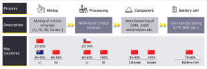
EY research shows China’s hold over processing of EV components encompasses 80-90% of global share. At the same time with giants like CATL, China houses over 70-80% of global LIB manufacturing. Over the years these giants have innovated and reduced the use of Nickel and Cobalt in LIBs and produced Lithium iron phosphate (LFP) batteries on a large scale.
NMC batteries, which are still prevalent in the US and Europe provide an energy density advantage over the LFP batteries, which are in turn cheaper and are widely used in China. The energy density of LFP battery packs is about one-fifth lower by mass (Wh/kg) and one-third lower by volume (Wh/L) than that of NMC battery packs. This advantage, however, is partly offset by LFP’s capability to reach 100% state of charge when required without significant degradation, whereas NMC batteries are typically limited to 80% to preserve long-term performance. The NMC batteries are preferred for operating in colder climates and over long ranges. Whereas enhanced performance level of LFP batteries and the given cost advantages have made them popular in the mass markets.
Global Lithium Constraints:
Primarily Lithium, often referred as ‘white gold’ is extracted from two sources across the globe. Firstly, there are minerals like spodumene, petalite, and lepidolite and secondly from Lithium salts like Lithium hydroxide, Li carbonates and Li chlorides which are highly available in lakes across the Andes mountains.
Parts of Argentina, Bolivia and Chile form the Lithium triangle with large proportion of world’s Lithium reserves. However, an nationalization drive over these reserves seems to proliferate in the Latin American countries, akin to what took place vis-à-vis oil sector with the formation of OPEC in the 1960s introducing new complexities on global supply chains.
Then there is also research going on Absorption type aluminium based direct Lithium extraction, which can reduce water drainage, but such methods are at low Technical Readiness levels (TRL)
Finding a way around the ‘White Gold’:
These dynamics have compelled governments and automakers to look at alternatives to Lithium. Some of the alternate EV battery technologies considered are as follows:
| Battery Technology | Anode Active Material (AAM) | Cathode Active Material (CAM) | Electrolyte |
| Sodium Ion Battery (SIB) | Hard as well as soft Carbon easily available from Crop residue or Agri waste | Sodium ions such as layered oxides | Salts such as sodium hexafluorophosphate (NapF6) |
| Zinc manganese Dioxide battery | Zinc metal, 80% of which globally available is from recycled products | Oxygen from air | Aqueous solution of Potassium hydroxide
(KOH) |
| Aluminium-Air battery | Solid Aluminium metal | Oxygen from air | High pH solution of KOH, NaOH or even NaCl. |
| Hydrogen Fuel Cell (HFC) | Hydrogen gas | Oxygen from air | KOH or NaOH |
The metals other than Lithium that are mostly used in metal ion or metal air batteries are widely available but TRLs of 7-9 as required for commercial EVs are yet not achievable with these technologies. However, technologies like Al-air batteries are inducted in other applications like medical devices. Metal air batteries have higher energy density and lower cost than LIBs but have persistent design challenges.
Batteries with solid electrolytes called solid state batteries are looked upon with high optimism even with low TRLs. Electrolytes used in them are mostly oxides, sulphides or polymer electrolytes.
While HFCs are in use commercially, but their production methods remain debatable. Production of hydrogen through electrolysis of water called green hydrogen is still limited compared to blue hydrogen (produced from methane) and grey hydrogen (produced from capturing hydrogen from fossil fuel).
Reducing Dependence through Recycling
A major source of Raw material extraction is Urban mining, which involves extracting valuable materials from E-Waste contributing to a circular economy. According to Global E-waste monitor, we might see E-waste production levels of 82 million tonnes globally by 2030 providing huge recycling potential. Although inefficient recycling mechanisms hinder urban mining potential. A systematic process of collecting, sorting and dismantling E-waste followed by methods like Pyrometallurgy (Smelting), Hydrometallurgy (Chemical separation) and Biometallurgy (Biological separation) must be integrated at ground level.
It is to be remarked that Alternative battery solutions won’t reduce the share of LIBs and LFPs in EVs immediately just as EVs won’t suddenly replace ICEs on roads. A coordinated strategy working on conventional sources while building resilience through alternatives is the need of the hour for a just climate transition.
The post Road to Alternate Battery Solutions: Beyond Lithium for a Sustainable Future appeared first on ELE Times.
Reimagining Human-Machine Interaction: Force Sensing as the New Frontier in HMIs
Introduction- From Mechanical Inputs to Force-Sensitive Interfaces
Human–Machine Interfaces (HMIs) have transformed dramatically in the past few decades. Early systems relied on mechanical switches, levers, and tactile buttons, robust but limited in design flexibility. The capacitive touch revolution brought sleek glass panels, multi-touch gestures, and sealed surfaces to smartphones, automotive dashboards, and industrial equipment.
However, capacitive technology has well-known drawbacks: poor performance in humid environments, false triggers, difficulty working with gloves, and limited ability to distinguish intentional versus accidental touches. Engineers have long sought the next leap in interaction technology.
That leap is force sensing the ability of HMIs to detect not just whether a surface is touched, but how firmly it is pressed. This evolution unlocks richer interaction, robust operation across challenging environments, and freedom from restrictive material choices. As Dr. Mark Weiser, often regarded as the father of ubiquitous computing, once said:
“The most profound technologies are those that disappear. They weave themselves into the fabric of everyday life until they are indistinguishable from it.”
Force sensing is enabling precisely this an interaction layer so intuitive and adaptable that it becomes invisible, yet indispensable.
Technology Fundamentals- How Force Sensing Works
Force sensing is fundamentally about converting mechanical load into an electrical signal. Two primary sensing principles dominate the market: piezoresistive and capacitive force sensing.
Piezoresistive Force Sensors
- Operate by measuring a change in electrical resistance when a material deforms under load.
- Typically use a full-bridge Wheatstone configuration, where four resistive elements form a balanced circuit.
- When force is applied, resistance changes unbalance the bridge, producing a measurable voltage signal.
- Advantages: High sensitivity, strong signal-to-noise ratio (SNR), good temperature compensation, suitability for MEMS fabrication.
- Considerations: Requires calibration to account for long-term drift and environmental conditions.
Capacitive Force Sensors
- Detect changes in capacitance caused by the displacement of conductive plates.
- Well-suited to applications where transparency or minimal deformation is required.
- Limitations: Susceptible to interference from humidity, dust, and certain materials; reduced performance with thick overlays.
MEMS Integration- Driving Miniaturization and Reliability
MEMS (Micro-Electro-Mechanical Systems) fabrication has transformed force sensing by enabling:
- Micron-scale sensing elements for compact integration.
- Tight tolerances and reproducibility, ensuring low hysteresis and predictable linearity.
- On-chip integration of low-noise amplifiers (LNA) and analog-to-digital converters (ADC), minimizing latency and reducing PCB real estate.
- Lower power consumption, which is vital for battery-powered devices.
By combining the sensing element, amplifier, and ADC into one package, designers can reduce complexity, improve EMC (Electromagnetic Compatibility), and speed up time-to-market.
Engineering Performance Metrics
Top engineers evaluating force sensors look beyond basic operation and focus on specific metrics:
- Sensitivity- The smallest detectable change in force; expressed in mV/V/N or equivalent.
- Linearity-The degree to which output correlates proportionally with applied load across the sensing range.
- Hysteresis– Difference in output between loading and unloading at the same force; lower values mean more repeatable performance.
- Power Consumption– Measured in µW or mW; critical for mobile and IoT devices.
- Temperature Stability– Resistance to thermal drift over wide operational ranges.
- Latency– The delay between applying force and obtaining a usable output; must be minimal for real-time feedback systems.
- Durability and Fatigue Life– How well the sensor maintains calibration after repeated load cycles.
Reference Example- Qorvo’s Integrated Force Sensor
Qorvo’s full-bridge piezoresistive MEMS force sensor exemplifies current best practice in integration:
- Architecture: MEMS sensing die + low-noise amplifier + on-chip ADC.
- Performance: Sensitivity up to 50× that of traditional capacitive sensing.
- Thermal Stability: Full-bridge layout compensates for temperature-induced resistance changes.
- Size: Compact footprint for easy integration in constrained spaces.
- Noise Reduction: Common-mode noise rejection inherent to Wheatstone bridge design improves measurement reliability.
This level of integration reduces external component count, simplifies PCB layout, and delivers predictable performance across demanding environments such as automotive cabins or factory floors.
Capacitive vs. Force Sensing – A Technical Comparison
| Aspect | Capacitive Sensing | Force Sensing |
| Pressure Detection | Detects touch only | Detects both light and firm presses |
| Material Options | Requires conductive/transparent surfaces | Works through metal, wood, plastic |
| Environmental Resistance | Sensitive to moisture, gloves, humidity | Performs in wet, dusty, or extreme conditions |
| False Triggers | Higher risk in contamination | Lower, needs deliberate pressure |
| Durability | Surface wear impacts function | Can be sealed for long service life |
Integration Considerations for Engineers
Force sensing delivers new possibilities, but integration requires careful planning:
- Overlay Material– The stiffness, thickness, and elasticity of the cover layer affect force transfer and sensor response.
- Mechanical Coupling– Poor coupling between the overlay and sensor leads to inconsistent readings.
- Calibration & Compensation– Initial factory calibration and in-field software compensation mitigate drift and account for production tolerances.
- Signal Conditioning– Filtering and amplification tailored to the application’s dynamic range are essential for maintaining high SNR.
- Power Management– Sleep modes, duty cycling, and event-driven activation preserve battery life in portable designs.
- Interface Protocols– Support for standard digital interfaces (I²C, SPI) ensures compatibility with a wide range of MCUs and SoCs.
Application Spectrum
Force sensing’s unique combination of precision, environmental resilience, and material flexibility makes it valuable across sectors:
1 Automotive
- Smart dashboards without mechanical buttons.
- Steering wheel controls that differentiate between light navigation and firm command inputs.
- Surfaces resistant to dust, vibration, and thermal cycling.
2 Wearables & Consumer Electronics
- Waterproof, gapless designs that still respond to fine pressure variations.
- Wearables that maintain tactile accuracy under sweat, rain, or glove use.
3 Industrial Controls
- Equipment interfaces operable with gloves, in oily or dusty conditions.
- High durability in mission-critical control systems.
4 Medical Devices
- Sterile, sealed surfaces for hospital environments.
- Precise force detection for surgical robotics and diagnostic equipment.
Market Dynamics & Growth Drivers
The demand for rugged, low-maintenance HMIs is accelerating, driven by:
- Industry 4.0 and increased automation.
- Automotive electrification, requiring cleaner, smarter control surfaces.
- Wearable health tech, where reliability and waterproofing are paramount.
- IoT proliferation, pushing for sensors with low power consumption and high integration.
Future Directions
Force sensing is evolving toward multi-modal, adaptive HMIs:
- AI-Assisted Sensing– Systems that learn individual user habits, adjusting sensitivity dynamically to reduce false positives.
- Sensor Fusion– Combining force sensing with capacitive, optical, and haptic elements for richer interaction profiles.
- Standardization Efforts– Creating performance benchmarks and interoperability guidelines to accelerate adoption.
- Ultra-Low-Power Designs– Extending sensor battery life into multi-year ranges for IoT nodes.
Conclusion-Toward a New Input Paradigm
Force sensing is not just a technical upgrade, it fundamentally changes how devices interpret human intent. For engineers, it represents:
- Greater control over input granularity (light vs. firm presses).
- The ability to design HMIs for challenging environments without sacrificing aesthetics.
- Reduced maintenance through sealed, wear-resistant surfaces.
As the technology matures, the combination of MEMS precision, integrated signal processing, and intelligent software adaptation could make force sensing a standard HMI layer in everything from cars to medical devices. In many cases, the future of interaction will not be whether a device was touched but how it was touched.
The post Reimagining Human-Machine Interaction: Force Sensing as the New Frontier in HMIs appeared first on ELE Times.
Transforming EVs at AutoEV Bharat 2025 – High Efficiency Power Electronic
Power electronics is the silent engine behind every electric vehicle for regulating and controlling the electrical flow powering motors and providing a level of drive.
AutoEV Bharat 2025 showcases the innovations in power electronics that make EVs more efficient, smaller, and better performing.
Inverters and converters lie in the heart of these technologies, the power electronics that convert DC power from the battery into AC power for the motor. By doing so, they allow exact control of the motor speed and torque, resulting in smooth acceleration, power-efficient energy use, and superb driving experience.
Today, an EV demands a high-density, compact level of power electronics. AutoEV Bharat 2025 highlights next-generation designs that shrink the size and weight of these components while maintaining power ratings. Smaller size, then, results in more space and better thermal efficiency, thus aiding in vehicle packaging.
Advanced motor controllers are coupled with these power electronics to dynamically control torque, regenerative braking, and direction of power. Based on predictive algorithms, these systems optimize performance under multiple driving situations, such as city stop-and-go, highway, and hilly terrain.
Efficiency gain due to state-of-the-art power electronics leads to extended battery life and driving range. Less energy is lost upon conversion, and hence the vehicles can cover longer distances in a single charge; simultaneously, heat management systems work against overheating and help in extending component life.
Being future-ready, power electronics showcased at AutoEV Bharat 2025 empower rapid charging, bidirectional energy flow, and energy exchange with the grid. These include Vehicle-to-Grid (V2G) operations, where EVs are in a state to discharge some energy back into the grid at times of peak demand, on-demand turning the vehicles into mobile energy reservoirs.
AutoEV Bharat 2025, in its attempt to develop compact, high-performance, and intelligent power electronics, sets up India’s EV ecosystem for obtaining world-class efficiency, equally smooth driving dynamics, and smart energy system integration.
The post Transforming EVs at AutoEV Bharat 2025 – High Efficiency Power Electronic appeared first on ELE Times.
Exploring the Triggers of Trade Wars and Their Global Economic Impact
The recent imposition of tariffs on India by the United States has sent shockwaves through various industries and economies across the globe. With the ongoing trade war between the two countries, the impact of these tariffs is being felt far and wide. The tariff war between two big economies will have long-term effects on the world economies.
By increasing the cost of imported goods from India, US consumers may end up paying higher prices for products. This could lead to a decrease in consumer spending and ultimately slow down economic growth. Moreover, retaliatory measures from India could further escalate the trade war and result in a tit-for-tat cycle of tariffs. It could also set a dangerous precedent for protectionist measures by other countries.
The real cause of the US tariff imposition on India and a probable policy shift could be attributed to a combination of factors, including Dollar crisis, arms lobby in the United States, massive debt and the personality clash between the leaders.
The arms lobby in the United States is a powerful force that plays a significant role in shaping the country’s foreign policy, including trade relations with other countries. One of the main factors could be the massive $32 trillion debt that the US currently faces. In an effort to raise the country out of its economic crisis, the US government has resorted to imposing tariffs on imports.
With the economic crisis looming large, the US government is looking for ways to boost its economy and reduce its debt burden. By imposing tariffs, the US aims to protect domestic industries and create more job opportunities for its citizens. This move is part of a larger strategy to revive the US economy and reduce its dependency on foreign goods.
The imposition of tariffs by the United States has sparked debates and discussions about the real motives behind such actions. In case of India, the real cause of US tariff imposition goes beyond just trade imbalances and economic competitiveness.
One of the main reasons is to curb the rapid economic growth and development of Bharat, the country has been experiencing in recent years. India’s booming economy, skilled workforce, and expanding market have made it a significant player in the global arena. This rapid progress poses a potential challenge to the long-standing economic supremacy of the United States. The US may feel threatened by India’s economic growth and global influence.
One of the main concerns regarding the US tariff imposition on India is the unpredictable nature of President Trump. As a fickle-minded person, Trump has been known to change his stance on tariffs and trade policies frequently, which can create uncertainty in the global market. This unpredictability can make it difficult for businesses to plan for the future and invest in long-term projects. U.S. trade policies will likely slow down global economic growth and rekindle inflation in the United States, where there is at least a 40% probability of a recession in the second half of this year.
India can take proactive steps to address the issue of US tariffs and mitigate their impact on the economy. This includes engaging in dialogue with US officials to resolve trade disputes, diversifying export markets to reduce reliance on the US, and investing in domestic industries to boost competitiveness. Additionally, India can explore opportunities for collaboration and partnerships with other countries to counter the effects of unilateral US actions. Experts widely agree that India’s overall macro picture remains stable, thanks to its inward-focused economy, diverse export markets, and domestic demand resilience.
Devendra Kumar
Editor
The post Exploring the Triggers of Trade Wars and Their Global Economic Impact appeared first on ELE Times.
AutoEV Bharat 2025: Solid-State Batteries and the Energy Revolution Ahead
Being the very core of electric mobility, the battery is the centre of attention at the AutoEV Bharat 2025. The exhibition platform showcases breakthrough technologies that seek to address today’s major issues: cost, safety, and performance and of course the technology.
Among them are solid-state batteries, purported to have a higher energy density than the conventional lithium-ion type, as well as faster charging and thermal stability faintly-contradicting-these-traditional Li-ion’s-stated-weaknesses. Startups, research labs, and manufacturers in India are demonstrating pilot-scale production models with the potential of increased safety and extended EV range.
A special highlight has been given to battery-swapping solutions that aim to support delivery fleets, e-rickshaws, and buses. Swappable packs with standardization allow for quick turnaround times and very economically viewed by the operation, thereby allowing for mass fleet electrification.
Another key area is AI-driven battery management solutions. These intelligent solutions optimize charge-discharge cycles, predict degradation, and maintain health in real time, which is critical for temperatures such as India has-hot, humid, and high temperature during the day and dropping drastically during the night.
The other defining theme at the AutoEV Bharat 2025 is AI-driven Battery Management Systems (BMS). Intelligent monitoring of charge-discharge cycles, predictive analytics for battery degradation, and real-time health checks are becoming vital in India’s hot and humid climate. Exhibitors will demonstrate how these technologies not only extend battery life but also provide safety assurance and better consumer confidence.
Since sustainability is also a central theme of AutoEV Bharat 2025, India must come up with proper frameworks for battery recycling and a second life given the world move toward circular economies. Recycling companies and energy startups will show how lithium, cobalt, and nickel are recovered from used cells. Retired EV batteries will be almost simultaneously implemented in grid storage systems supporting the integration of renewable energy resources, such as solar and wind, into India’s power networks.
AutoEV Bharat 2025, incorporates that batteries are no longer just components they emerge as enablers for a full mobility transformation. While nurturing everything from the coolest solid-state cells to the most practical battery swap models, this show comes as a meeting point for the industry to collaborate, innovate, and steer the journey of EV in India forward.
For policymakers, AutoEV Bharat 2025 provides needs for technology concerning support around infrastructure and regulation. For entrepreneurs, the occasion waves opportunities around localization, supply chain innovation, and global partnership. For consumers, it is reassurance that the EVs of tomorrow will be safer, longer-lasting, and more affordable.
As India gears up to lead the world in sustainable mobility, AutoEV Bharat 2025 stands as the stage where the future of battery technology is not just imagined, but experienced.
The post AutoEV Bharat 2025: Solid-State Batteries and the Energy Revolution Ahead appeared first on ELE Times.
Acopian Unwraps 900 W Low Profile AC-DC Power Supply
My favorite new tool in the lab: Washi paper tape cutters
 | Saves me having to always read for scissors or a bulky tape dispenser taking up valuable desk space. I had ordered one online and picked up a few more on my recent holiday to Japan. [link] [comments] |
SoC extends IoT range with efficient sub-GHz radio

Joining Silicon Labs’ sub-GHz wireless SoC family, the FG23L delivers secure long-range connectivity for resource-constrained IoT devices. Its link budget of ~146 dB and transmit power of +20 dBm provide up to twice the range of comparable devices. By balancing performance and affordability, the SoC broadens sub-GHz adoption across markets from industrial automation and smart city infrastructure to agriculture IoT and connected homes.

The FG23L runs on a 78-MHz Arm Cortex-M33 with DSP extensions and an FPU for efficient signal processing. It includes 128 KB of flash and 32 KB of RAM to support application and data storage. The low-power radio core spans the full range of license-free sub-GHz ISM bands (110 MHz to 970 MHz). Active and sleep currents of 36 µA/MHz and 1.2 µA, respectively, enable over 10 years of battery life.
Midlevel Secure Vault safeguards the communication channel and defends against logical attack vectors. Security features include a true random number generator, crypto engine, secure application boot, and secure debug lock/unlock.
The FG23L will be generally available on September 30, 2025. Developer kits are available now.
The post SoC extends IoT range with efficient sub-GHz radio appeared first on EDN.
In-plane Hall switch rivals MR sensors

The TMAG5134 in-plane Hall-effect switch from TI offers a cost-effective alternative to magnetoresistive (MR) sensors for position sensing. An integrated magnetic concentrator enables detection of magnetic fields as weak as 1 mT in door and window sensors, home appliances, and personal electronics. Its in-plane sensing adds design flexibility by detecting magnetic fields parallel or horizontal to the PC board.

Designers typically do not consider Hall-effect switches as viable replacements for reed switches or tunnel, anisotropic, and giant MR sensors because of their limited sensitivity. The TMAG5134 overcomes this limitation, delivering higher sensitivity than conventional Hall-effect sensors without the added cost and complexity of MR devices.
Operating from a 1.65-V to 5.5-V supply, the TMAG5134 consumes just 0.6 µA on average. Its magnetic concentrator amplifies the sensor signal, eliminating the need for additional bias current. The device offers flexible magnetic pole detection (omnipolar or dual-unipolar) and is available with push-pull or open-drain outputs, in both active-low and active-high configurations. Magnetic operating points range from 1 mT to 2 mT for versatile position-sensing applications.
Manufactured in TI’s advanced 300-mm fabs, the TMAG5134 is available in production quantities on TI.com.
The post In-plane Hall switch rivals MR sensors appeared first on EDN.
200-V MOSFETs offer high-efficiency design

iDEAL Semiconductor has announced its first family of 200-V MOSFETs based on high-performance SuperQ technology. The SuperQ architecture increases silicon utilization from 50% to 95%, increasing efficiency, reducing energy losses, and improving cost-performance. It also preserves silicon’s core advantages: ruggedness, high-volume manufacturability, and reliability up to 175 °C.

Now in mass production, the iS20M028S1P is a 25‑mΩ N‑channel MOSFET in a TO‑220 package. It offers a wide safe operating area and high current capability, handling continuous currents up to 40 A. All units are 100% UIS tested in production to ensure reliability. Low switching losses improve efficiency, while a 26.5-nC gate charge and +0.5-V gate-threshold variation make paralleling simpler.
Devices with the lowest resistance, available for sampling in TOLL and D2PAK‑7L packages, achieve a maximum on-resistance of just 5.5 mΩ—1.2× lower than the current market leader and 1.7× lower than the next-best competitor, according to iDEAL.
Applications for the 200‑V SuperQ family include motor drives, LED lighting, battery protection circuits, AI servers, isolated DC/DC power modules, USB‑PD adapters, and solar power systems.
Datasheets and a full list of available part numbers, including the sampling devices, can be found here.
The post 200-V MOSFETs offer high-efficiency design appeared first on EDN.
Frequency extenders boost VNA range to 250 GHz

Keysight’s NA5305A and NA5307A mmWave modules extend PNA and PNA-X vector network analyzers (VNAs) to 170 GHz and 250 GHz, respectively. Paired with the 85065A 0.5-mm coaxial calibration kit and N5292A test set controller, the frequency extenders enable fully calibrated single-sweep broadband S-parameter measurements from 100 kHz (or 10 MHz) up to 250 GHz.

The broadband VNA accessories simplify test setups and enable engineers to characterize on-wafer or packaged components at sub-THz frequencies. They also help accelerate the design and validation of 1.6‑Tb/s and 3.2‑Tb/s components and next-generation semiconductors.
Test configurations provide a dynamic range of 105 dB at 170 GHz for passive components, high-rejection filters, and active devices. Differential measurements help validate active devices and high-speed interconnects, with maximum output power of 0 dBm at 170 GHz and –5 dBm at 220 GHz.
Existing 110‑GHz and 120‑GHz VNA users can easily upgrade their configuration to preserve their original investment.
The post Frequency extenders boost VNA range to 250 GHz appeared first on EDN.
RISC-V IP expands AI capabilities at the edge

SiFive’s Intelligence Gen 2 RISC-V IP portfolio combines scalar, vector, and matrix compute to accelerate AI workloads. The Gen 2 lineup includes the new X160 and X180, alongside the upgraded X280, X390, and XM series. All products feature enhanced scalar and vector processing, while the XM series adds a highly scalable matrix engine.

With up to four cores, the 32-bit X160 and 64-bit X180 target embedded IoT at the far edge. They deliver high efficiency in a compact footprint, extending AI to automotive, robotics, and industrial automation. Their vector engine boosts AI model performance with minimal power and area overhead.
Intelligence Gen 2 products span a wide range of performance, area, and power options within a single scalable Instruction Set Architecture (ISA). Features include a dual-issue, in-order eight-stage superscalar pipeline, narrow-to-wide vector engines, and the XM series’ scalable matrix engine for diverse AI workloads. The CPUs also support the SiFive Scalar Coprocessor Interface (SSCI) and Vector Coprocessor Interface eXtensions (VCIX) to link external AI accelerators and coprocessors.
All five Intelligence Gen 2 products are now available for licensing, with first silicon expected in Q2 2026.
Intelligence Gen 2 product page
The post RISC-V IP expands AI capabilities at the edge appeared first on EDN.
Between two vendors

It was a classic stand-off. Vendor number one’s system wasn’t talking to vendor number two’s. What to do? Of course! Blame the customer’s network!
I worked for a TV station that was part of a group run by a common owner. One of the stations in the group used a system known as production automation, which allowed a single operator to control all of the equipment in the control room during newscasts. That would include the video switcher, audio console, camera robotics, video playback, lighting, and graphics generators. The computer system in the newsroom takes the scripts written by reporters and producers, generates a sequence called a rundown, and transmits and updates it in real-time to the automation system.
Do you have a memorable experience solving an engineering problem at work or in your spare time? Tell us your Tale
While performing a major update to one of the systems, communication stopped. Head scratching ensued for a while, and then the two vendors decided the problem must be something in the network that was blocking the IP packets. The station’s engineers pointed out that nothing had been changed in their network, and in any case, there was no internal routing or filtering going on. Not good enough, say the vendors. Prove to us it’s not your fault before we continue. Their advice was to install a copy of Wireshark, analyze the packets, and show us that the path between the systems is clear.
That’s reasonable as far as it goes, but Wireshark is a mighty powerful tool, and it is not for the faint of heart. At the local TV station level, the IT staff generally does not have the expertise needed to fire it up quickly and interpret its results. The station group’s central IT networking folks do, but getting them involved would have taken a good deal of time, and if they had to travel to the site, expense.
I was just a bystander to this. My own station was one of those with the same systems, so I was included in all of the emails flying back and forth. As it happens, not long before this incident, I had written a small one-trick pony Windows utility. All it did was send IP packets from one computer to another via a specific port. As seen in Figure 1, if the path is clear, the receiving computer replies, and the arrows move. Simple as that.

Figure 1 A demonstration of the Windows utility written by the author, sending IP packets from one computer to another via a specific port.
I sent the program to the station’s IT director, and in less than half an hour, he installed it on both systems, checked all of the ports the vendors specified, and found them all clear. With no more finger-pointing at the customer, the vendors had to get to work to find the actual cause of the problem, which turned out not to be network-related.
A few notes about the program. The image shown is just a demonstration, with both ends running on the same machine. In real life, one copy would be on each of two machines on the network, across the room, or across the world. Also, to be honest, I probably spent more time getting the ballistics of the arrow movement looking good than on the rest of the program.
Robert Yankowitz retired as Chief Engineer at a television station in Boston, Massachusetts, where he had worked for 23 years. Prior to that, he worked for 15 years at a station in Providence, Rhode Island.
Related Content
- The mysterious MS-DOS reboot
- TV transmitter trouble
- A network-protocol primer
- IP Resilient Network Fundamentals–Part III
The post Between two vendors appeared first on EDN.
Сторінки


![[link]](https://i.redd.it/r9gyxbw3dqof1.jpeg)