
ELE Times

Asia-Pacific Takes the Lead in AI Adoption Across Manufacturing
Courtesy: Rockwell Automation
Manufacturing around the world has undergone a significant transformation with the emergence of artificial intelligence (AI) and machine learning. With dynamic market conditions and pressures to optimize operations across the supply chain, more businesses today are turning to technology to meet the demands of an increasingly competitive market.
To get a better understanding of the smart manufacturing landscape and how manufacturers are leveraging these new technologies, the latest edition of the State of Smart Manufacturing report (SOSM) surveyed more than 1,500 manufacturing decision makers across industries from 17 countries, including Asia Pacific nations Australia, China, India, Japan, New Zealand, and South Korea.
Now in its 10th edition, the report offers a global perspective on today’s challenges and tomorrow’s opportunities, highlighting how smart manufacturing and emerging technologies are fostering resilience and shaping the future.
How AI is Challenging the Status Quo in the Asia Pacific
Rich in resources with the resilience to constantly adapt and innovate, Asia Pacific (APAC) is setting the pace for manufacturing and industrial growth around the world. There is strong digitization momentum across the region, as AI and smart manufacturing technologies are no longer buzzwords but have become mission-critical to drive quality, agility, and growth.
This year’s survey is proof that the focus has shifted from experimentation to execution, where more manufacturers have adopted a tech-first mindset. Nearly half of manufacturers are already scaling AI to address workforce gaps, cybersecurity risks, and evolving sustainability targets, and APAC organizations investing in generative and causal AI increased 10% year-over-year.
The growing maturity in how businesses view AI is noticeable, moving towards becoming a strategic enabler rather than a supplementary tool. Trust in AI has deepened, with 41% of those surveyed in APAC having plans to increase automation in the workplace to address workforce shortage and bridge the skills gap. Organizations are no longer primarily using AI for predictive maintenance. They are now leveraging these capabilities for other, more sophisticated, autonomous operations such as quality assurance and adaptive control, which help to reduce human error and enhance real-time decision-making.
AI in Cybersecurity
With the rapid adoption of digital technologies, cybersecurity has become a growing concern across industries, including manufacturing. Globally, it now ranks as the second most significant external obstacle for manufacturers. In the APAC region, cybersecurity is top of the list, alongside inflation and rising energy costs.
In response, businesses are accelerating their use of AI, adopting smart manufacturing technologies to digitize operations, and upskilling existing talent to stay competitive and minimize cybersecurity risks. They are also hiring with new priorities, whereby cybersecurity skills and standards have become an in-demand capability.
Understanding the need for secure-by-design architectures and real-time threat detection capabilities, Rockwell Automation has developed a series of threat intelligence and detection services, helping manufacturers to stay ahead of the evolving cybersecurity frameworks and industry standards.
Transforming the Workforce with AI
Alongside AI, the workforce, too, is evolving. Just as AI can support business needs, it requires a skilled workforce to adapt these technologies to deliver real business value. Manufacturers across APAC are looking to AI to increase automation and make workflows more efficient, while looking for employees with strong analytical thinking skills to take on more value-added tasks. While challenging, the SOSM report reveals that the need for more skilled workers is not a uniquely regional issue but a global concern, affecting industries in both developed and emerging markets.
On the upside, the skills gap in APAC has narrowed slightly from the previous year, with only 29% of respondents in 2025 citing skills gap as a challenge compared to the 31% in 2024. This suggests that investments in talent development and education are beginning to pay off.
Delivering More Sustainable Business Outcomes for the Long Run
As an industry, manufacturing consumes lots of energy. As manufacturers across the region become more invested in their ESG goals, they are driven to improve business efficiencies in pursuit of sustainability and resource conservation. Over half (55%) stated that improving efficiencies is the top reason to pursue better sustainability, up from 39% last year. By improving workflow efficiencies through automation and technologies like AI, businesses are saving on business costs while supporting better energy management.
As the 2025 State of Smart Manufacturing report shows, AI is no longer a distant promise for the Asia Pacific—it is a powerful catalyst actively reshaping how the region builds, protects, and grows. From strengthening cybersecurity and elevating workforce capabilities to enabling smarter energy use and more sustainable operations, APAC manufacturers are demonstrating what it means to move from digital ambition to digital action.
With technology adoption accelerating and confidence in AI deepening, the region is well-positioned to define the next era of global manufacturing. Those who continue to invest in talent, innovation, and secure, future-ready systems will not only overcome today’s challenges but also lead the transformation of industry for years to come.
The post Asia-Pacific Takes the Lead in AI Adoption Across Manufacturing appeared first on ELE Times.
Will AI Consume the World’s Electricity? Addressing AI Data Center Demands with Advanced Power Semiconductors
Courtesy: RoHM
AI’s unprecedented advancement is reshaping our world, but this transformation comes with the urgent challenge of sharply rising energy demands from data center infrastructure.
In response, Japan has launched an ambitious national strategy—the ‘Watt-Bit Initiative’—spearheaded by the Ministry of Economy, Trade, and Industry (METI). This comprehensive program aims to establish Japan as a global leader by developing ultra-efficient data centers strategically distributed across the nation. Through collaborative platforms like the ‘Watt-Bit Public-Private Council,’ METI is orchestrating a unified effort among key sectors—energy providers, telecommunications, data center operators, and semiconductor manufacturers—to turn this vision into reality.
Will AI Consume the World’s Electricity?
The explosive growth of generative AI technologies like ChatGPT has triggered an unprecedented surge in data center energy demands. Training and inference of complex AI models require enormous computational resources, supported by high-performance servers operating continuously around the clock.
This escalating demand for electricity not only places a significant strain on local environments but also raises concerns about the stability of the power supply. As AI continues to advance, the limitations of conventional power supply systems are becoming increasingly apparent.

Against this backdrop, three urgent challenges emerge: improving energy efficiency, expanding the use of renewable energy, and optimizing the regional distribution of data centers. Achieving a sustainable society requires moving away from fossil fuel dependency and embracing renewable sources such as solar and wind power.
Utilizing Renewable Energy in Data Centers
Data centers, now an indispensable part of modern infrastructure, are at a major turning point.
Traditionally, urban data centers have been concentrated in metropolitan hubs like Tokyo to ensure low-latency communication for services requiring high-speed data access, including finance, healthcare, and edge computing. However, the surge in power consumption driven by AI adoption, coupled with the need for robust business continuity (BCP) in the face of large-scale natural disasters, is accelerating the shift toward decentralizing data centers into suburban areas.

These new sites offer compelling advantages beyond just abundant available space. They enable seamless integration of renewable energy sources such as solar and wind power, benefit from surplus grid capacity for stable electricity, and leverage natural cooling from climate and water resources, dramatically reducing operational costs. As a result, suburban facilities are increasingly being adopted for modern workloads such as cloud hosting, backup, disaster recovery, and large-scale storage.
The Future of Server Rack Expansion
Urban data centers face severe land constraints, and even suburban data centers, where securing large plots is relatively easier, are approaching their limits in available space for server deployment.
To overcome this, server racks are evolving into high-density AI server racks designed to house a greater number of high-performance servers efficiently. Rather than expanding the total number of server racks, the industry is moving toward high-density configurations equipped with more CPUs, GPUs, and other functional boards, significantly boosting the computing power per rack to maximize performance within limited space.
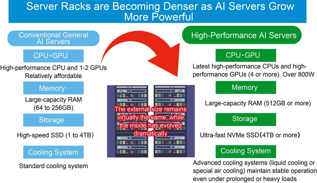
While the external appearance of server racks remains largely unchanged, their internal storage capacity has increased several fold.
This leap in performance and density demands a fundamental transformation of power delivery systems. Conventional multi-stage power conversion introduces significant energy losses, making efficient supply increasingly difficult. As a result, innovations such as reducing conversion stages and adopting high-voltage direct current (HVDC) architectures are gaining momentum, driving the need for SiC and GaN power semiconductors. ROHM, together with other industry leaders, is advancing technologies that support this transformation, enabling both higher performance and greater energy efficiency across entire data centers.
- Are Today’s Power Systems Sufficient?
The sharp rise in power consumption of high-performance AI servers—particularly GPUs—is forcing a fundamental redesign of existing data center power architectures. Conventional multi-stage power conversion incurs significant conversion losses, making efficient power delivery increasingly difficult.

In today’s data centers, high-voltage AC is supplied and gradually stepped down through multiple transformers and rectifiers before finally being converted into the low-voltage DC required by servers. Each stage of this process incurs losses, ultimately reducing overall efficiency. To address these challenges, data centers are expected to undergo key transformations aimed at enhancing both power conversion efficiency and reliability.
- Reducing Power Conversion Stages
A growing trend is the integration of multiple conversion processes—for example, converting high-voltage AC directly to DC, or stepping down high-voltage DC directly to the voltage used by servers. This approach significantly reduces the number of conversion steps, minimizing energy losses, enhancing overall system efficiency, and lowering the risk of failures.
- Supporting High-Voltage Input/High-Voltage Direct Current (HVDC) Power Supplies
Server rack input voltages are shifting from traditional low-voltage 12VDC and 48VDC to higher levels such as 400VDC, and even 800VDC (or ±400VDC). Operating at higher voltages reduces transmission current, enabling lighter busbar designs.
At the same time, the adoption of HVDC systems is gaining momentum. Unlike conventional AC-based architectures, HVDC delivers DC power directly to server racks, reducing the need for multiple AC/DC conversion stages. This approach enhances energy efficiency, enables more flexible power management and bidirectional transmission, and simplifies integration with renewable energy sources.
- Increasing Adoption of SSTs (Solid State Transformers)
Transformer equipment is evolving from traditional designs to SSTs (Solid State Transformers) that leverage semiconductor technology. SSTs are expected to play a key role in significantly miniaturizing conventional equipment.
- Growing Demand for SiC/GaN Power Semiconductors
Building high-efficiency, high-voltage power systems requires performance levels that exceed the capabilities of conventional silicon (Si) semiconductors. This has made SiC and GaN power semiconductors indispensable. These advanced devices enable low-loss, high-frequency, high-temperature operation under high-voltage input conditions, greatly contributing to both the miniaturization and efficiency of power systems.

Moreover, as these technologies advance, their benefits extend beyond power systems to individual devices within server racks, further improving overall energy efficiency.
ROHM is accelerating the development of solutions for next-generation servers. In addition to existing products such as SiC/GaN/Si IGBTs, isolated gate drivers, cooling fan drivers, SSD PMICs, and HDD combo motor drivers from the EcoSiC, EcoGaN, and EcoMOS series, we are also developing high-current LV MOS, isolated DC-DC converters, DC-DC converters for SoCs/GPUs, and eFuses.
Power Semiconductors Driving Next-Generation AI Data Centers
- SiC Devices Ideal for High Voltage, Large Current Applications
SiC devices are particularly well-suited for sets requiring high voltages and currents. As server rack input voltages continue to rise, conventional 54V rack power systems face increasing challenges, including space limitations, high copper usage, and significant power conversion losses.
By integrating ROHM’s SiC MOSFETs into next-generation data center power systems, superior performance can be achieved in high-voltage, high-power environments. These devices reduce both switching and conduction losses, improving overall efficiency while ensuring the high reliability demanded by compact, high-density systems.
This not only minimizes energy loss but also reduces copper usage and simplifies power conversion across the entire data center.
- GaN Devices that Provide Greater Efficiency and Miniaturization
While SiC excels in high-voltage, high-current applications, GaN demonstrates outstanding performance in the 100V to 650V range, providing excellent breakdown strength, low on-resistance, and ultra-fast switching.
AI servers process far greater volumes of data than general-purpose servers, requiring high-performance GPUs, large memory capacity, and advanced software. This leads to higher power consumption, making efficient cooling and thermal management increasingly critical.
To address these challenges, GaN HEMTs – capable of high-speed switching (high-frequency operation) – are being integrated into power supply units to minimize power loss. This delivers major gains in power conversion efficiency, translating to substantial energy savings, lower operating costs, and reduced environmental footprint.
What’s more, GaN devices offer high current density, enabling a size reduction of approximately. 30-50% compared to conventional silicon devices. This not only improves space efficiency in power supplies and chargers, but also simplifies thermal design.
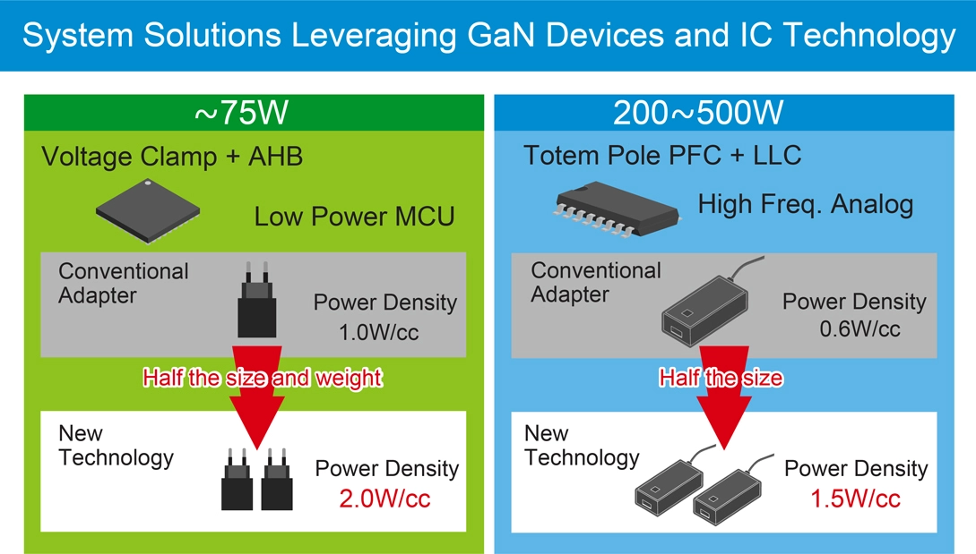
By reducing unit size and making effective use of freed-up space, the load on cooling systems can be alleviated, supporting overall system miniaturization and improved reliability. In addition, GaN’s high durability and suitability for high-frequency applications make it an ideal choice for data centers.
ROHM has succeeded in shortening the pulse width to as little as 2ns utilizing proprietary Nano Pulse Control technology, further enhancing the switching performance of GaN devices. Through the EcoGaN series, ROHM is expanding its lineup to meet the needs of AI data centers demanding compact, highly efficient power systems. The portfolio includes 150V and 650V GaN HEMTs, gate drivers, and integrated solutions that combine these components.
Conclusion
The evolution of AI, which shows no signs of slowing, comes with an inevitable surge in power demand.
According to the International Energy Agency (IEA), global data center electricity consumption is expected to more than double in the next 5 years, reaching approximately 945 billion kWh. Around half of this demand is projected to be met by renewable energy sources such as solar and wind, signaling a major shift in how energy is generated and consumed in the power-hungry data center sector. Technologies like photovoltaics (PV) and energy storage systems (ESS) are gaining traction as essential components of this transformation.
ROHM is actively contributing to this transition with a broad portfolio of advanced power semiconductor technologies, including SiC and GaN devices. These solutions enable high-efficiency power systems tailored for next-generation AI data centers. ROHM is also accelerating the development of new products to meet evolving market needs, supporting a more sustainable and prosperous AI-driven future.
The post Will AI Consume the World’s Electricity? Addressing AI Data Center Demands with Advanced Power Semiconductors appeared first on ELE Times.
STMicroelectronics streamlines smart-home device integration with industry-first Matter NFC chip
STMicroelectronics has unveiled a secure NFC chip designed to make home networks faster and easier to install and scale, leveraging the latest Matter smart-home standard. ST’s ST25DA-C chip lets users add lighting, access control, security cameras, or any IoT device to their home network in one step by tapping their phone. The chip is the first commercial solution fulfilling newly published enhancements in Matter—the latest open-source standard now making smart home devices secure, reliable, and seamless to use.
“The integration of NFC-based onboarding in Matter 1.5 is a timely enhancement to the smart home experience. Our market-first ST25DA-C chip leverages this capability to simplify device commissioning through tap-to-pair functionality. This reduces setup complexity, especially for installations that are difficult to access, thanks to NFC-enabled battery-less connectivity. This aligns well with the broader momentum in the smart home market to serve consumers who increasingly prioritize ease of use, interoperability, and security. NFC-enabled Matter devices are positioned to play a key role in driving even greater adoption,” said David Richetto, Group VP, Division General Manager, Connected Security at STMicroelectronics.
“Matter is an important standard for the smart-home industry, enabling seamless communication across devices, mobile apps, and cloud services. Its primary benefit is simplifying technology for non-expert consumers, which could help accelerate adoption of connected devices. The new STMicroelectronics’ ST25DA-C secure NFC chip is one example of next generation chipset that supports this standard, providing device makers with tools to develop the next generation of smart-home products,” said Shobhit Srivastava, Senior Principal Analyst at Omdia.
Technical information
Enhanced usability: ST’s new NFC Forum Type 4 chip significantly improves the user experience, leveraging NFC technology present in most smartphone devices. NFC-enabled device commissioning is faster, more reliable, and secure compared to conventional pairing using technologies such as Bluetooth® or QR codes, which are not always possible.
The ST25DA-C secure NFC tag can operate cryptographic operations required for Matter device commissioning using energy harvesting from the RF field. This mechanism allows users to jump-start adding unpowered devices to the smart home network. It also simplifies the installation of multiple accessories in parallel.
Focused on security: The ST25DA-C brings strong security to smart homes, leveraging ST’s proven expertise in embedded secure elements for protecting assets with device authentication, secure storage for cryptographic keys, certificates, and network credentials.
Based on Common Criteria-certified hardware, the ST25DA-C also targets certification to the GlobalPlatform Security Evaluation Standard for IoT Platforms (SESIP level 3).
The post STMicroelectronics streamlines smart-home device integration with industry-first Matter NFC chip appeared first on ELE Times.
Mitsubishi Electric India to Showcase Breakthrough Power Semiconductor Technologies at PCIM India 2025
Mitsubishi Electric India, is set to introduce its flagship cutting edge Power Semiconductor Devices and technology to the Indian market. MEI Participation in PCIM Asia New Delhi 2025 reinforces the company’s commitment on delivering high-efficiency semiconductor solutions to support India’s growing demand in the area of Home appliances, Railway, xEV, renewable energy and industrial Applications.
Visitors at PCIM India 2025 will experience the new DIPIPM platform that integrates inverter circuitry, gate-drive functions and protection features into a single module. These modules enable compact designs and improved system safety. Available in both IGBT and SiC-based versions, the latest Compact DIPIPM and SLIMDIP families are suited for applications such as room air conditioners, washing machines, commercial HVAC, solar pumping and light industrial drives.
Mitsubishi Electric India will also showcase a wider product portfolio, including high-voltage HVIGBT modules, LV100 and NX industrial power modules, and automotive-grade semiconductor platforms engineered for Utility-scale solar inverters, wind converters, EV charging & powertrains, Railway traction converters, HVDC transmission and induction heating. Alongside the Power Modules, Mitsubishi Electric India will also display its latest bare-die SiC MOSFETs and RC-IGBT technology which enables optimal structure, low loss, and high reliability devices for xEV- traction and charging applications.
| Product Line | Key Features |
| DIPIPM (Dual In-line Package Intelligent Power Module) | *Offers CSTBT & RC-IGBT chip technologies in a wide line-up *Available in 600V and 1200V, 5A–100A *Includes SiC-MOSFET variants and new Compact DIPIPM & SLIMDIP series |
| LV100 & NX Power Modules | *Industry-standard IGBT & SiC modules with 7th/8th gen CSTBT chipset and SLC packaging *Voltage: 1200V/1700V/2000V; Current: 225A–1800A *Includes new 8th gen LV100 & NX models |
| HVIGBT (High-Voltage IGBT) | *Modules for traction and power transmission *Voltage options: 1700V, 3300V, 4500V, 6500V; Current: 400A–2400A *High-voltage SiC up to 3300V/175A–800A *Includes new XB Series |
| Power Modules for Automotive | *Designed with integrated cooling fins and DLB technology *The Line-up of 2 in 1 circuit & 6 in 1 circuit with latest SiC & RC-IGBT chip technologies *Available in 750V/1300V, 350A–800A with on-chip current and temperature sensing *Includes new J3 Series |
Speaking on the participation, Mr. Hitesh Bhardwaj, General Manager/Business Head, Semiconductors & Devices, Mitsubishi Electric India said: “India is entering a decisive phase of Power Electronics across mobility, renewable energy infrastructure. With the introduction of latest Si and SiC semiconductor technologies to the domestic market, we aim to empower Indian manufacturers with smarter, more efficient and more reliable technologies. Our long-term vision is to support the country’s innovation ecosystem and contribute to sustainable growth across industry and society.”
With India’s manufacturing ecosystem evolving toward higher energy efficiency standards and smarter power architectures, Mitsubishi Electric India’s latest offering strengthens access to globally proven semiconductor innovation tailored for future-ready applications.
The post Mitsubishi Electric India to Showcase Breakthrough Power Semiconductor Technologies at PCIM India 2025 appeared first on ELE Times.
ASMPT Wins New Orders for Nineteen Chip-to-Substrate TCB Tools to Serve AI Chip Market
ASMPT announced it had won new orders for 19 Chip-to-Substrate (C2S) TCB tools from a major OSAT partner of the leading foundry serving the AI chip market.
ASMPT is the sole supplier and Process of Record (POR) of C2S TCB solutions for this customer, supporting their high-volume manufacturing requirements. These latest systems will enable their next-generation C2S bonding for logic applications as compound die sizes get larger. This demonstrates the customer’s continued confidence in ASMPT’s technological leadership and production-proven capabilities. Looking ahead, ASMPT is well-positioned to secure additional orders in the future.
This continued momentum for ASMPT’s flagship Thermo-Compression Bonding (TCB) solutions reinforces its position as the industry’s leading provider of advanced packaging solutions for artificial intelligence and high-performance computing applications.
“The TCB market is experiencing transformational growth driven by AI and HPC applications,” said Robin Ng, Group CEO, ASMPT. “Our comprehensive technology portfolio spanning chip-on-wafer, chip-on-substrate, and HBM applications positions ASMPT uniquely to support our customers’ most demanding advanced packaging roadmaps. This latest win validates our technology leadership and highlights the market’s recognition of our ability to deliver production-ready, scalable platforms.”
With the largest TCB installed base worldwide consisting of more than 500 tools, ASMPT is strategically positioned to capture between 35% to 40% of an expanded TCB market. ASMPT recently expressed confidence that the TCB Total Addressable Market (TAM) projection will exceed US$1 billion by 2027, bolstered by recent news about AI ecosystem investments.
The post ASMPT Wins New Orders for Nineteen Chip-to-Substrate TCB Tools to Serve AI Chip Market appeared first on ELE Times.
Microchip Halves the Power Required to Measure How Much Power Portable Devices Consume
Battery-operated devices and energy-restricted applications must track and monitor power consumption without wasting power in the process. To solve this challenge, Microchip Technology announced two digital power monitors that consume half the power of comparable solutions based on typical operating conditions at 1024 samples per second. The PAC1711 and PAC1811 power monitors achieve this efficiency milestone while also providing real-time system alerts for out-of-limit power events and a patent-pending step-alert function for identifying variations in long-running averages.
The 42V, 12-bit single-channel PAC1711 and 16-bit PAC1811 monitors are housed in 8- and 10-pin Very Thin Dual Flat, No-Lead (VDFN) packages, respectively, that are pin- and footprint-compatible with the popular Small Outline Transistor (SOT23)-8 package. This compatibility simplifies second-sourcing for developers, while streamlining upgrades and integration into existing systems.
“Until now, portable devices and a variety of energy-constrained applications have needed to burn a significant amount of valuable power to measure how much they are consuming,” said Keith Pazul, vice president of Microchip’s mixed-signal linear business unit. “Unlike many existing solutions, Microchip’s power monitors function as independent ‘watchdog’ peripherals, eliminating the need for the MCU to handle power monitoring tasks. These monitors allow the MCU or host processor to remain dormant until a significant power event occurs such as needing an LCD screen to power on.”
The PAC1711 and PAC1811 power monitors’ step-alert capability keeps a running average of voltage and current values. If there is a significant, user-defined variation, it will notify the MCU to act on it. The devices keep a rolling average, and any new sample can trigger an alert. A slow-sample pin option is available, which can delay the power usage sampling to every eight seconds and further conserve power.
An accumulator register in the power monitor can be used to manage logistical items, track system battery aging or time to recharge, and provide the short-term historical data for long-term power usage that the MCU can be programmed to act on. Both current monitor integrated circuits sense bus voltages from 0 to 42 volts and can communicate over an I2C interface. They are well-suited for first- or second-source options in computing, networking, AI/ML and E-Mobility applications.
The post Microchip Halves the Power Required to Measure How Much Power Portable Devices Consume appeared first on ELE Times.
India needs up to 15,000 crore more investment for PCB manufacturing: JS Gujral, MD, Syrma SGS
In the budget for 2021, the Indian government sanctioned Rs. 76,000 crores for the India Semiconductor Mission (ISM). Today, after nearly five years, there is a need for an additional investment of Rs. 10,000-15,000 crores in the next two to three years to boost domestic PCB manufacturing to reduce import dependency below 50%, according to JS Gujral, MD, Syrma SGS.
Currently, India demands PCBs worth nearly Rs. 50,000 crores, and only 10% of that demand is met locally, while the rest is fulfilled through imports from China, Taiwan and other nations. The aim is to increase the production to a worth of Rs. 20,000 in the next three years when the demand itself will rise to Rs. 70,000 worth.
From the many factors holding India back, the raw material bottle neck is a significant problem. Raw materials make up for nearly 60% of the total cost of the PCB. Copper Clad Laminate (CCL) is one of the primary materials used in PCB manufacturing. It covers nearly 27% of that raw material cost. While India is gradually progressing towards its complete domestic manufacturing, there are other burdens such as the copper foil, pre pregs, and specialized chemicals. These three are largely imported which add to the exorbitant costs of PCBs manufactured in India, making them costly and less competitive in the global market.
Experts recommend the increase in domestic supply for copper foils and necessary raw materials alongside CCL to maintain the competitiveness of locally produced PCBs to meet both national and international demands.
The post India needs up to 15,000 crore more investment for PCB manufacturing: JS Gujral, MD, Syrma SGS appeared first on ELE Times.
Slim DIN Rail Power Supplies For Industrial Applications
Advertorial by RECOM
DIN rail mounting has revolutionized electrical cabinets since the idea was first conceived in the 1920s to standardize the mounting of switchgear and enable interchangeability between manufacturers. DIN stands for “Deutsche Industrie Norm” or the “German Industrial Standard” and the success of the DIN rail system rapidly spread outside of Germany, eventually becoming the European standard DIN EN 60715.
The DIN rail system’s simplicity and versatility—allowing components to be easily clicked into place or removed for maintenance—has made it the preferred standard for electrical cabinet design. As a result, manufacturers offer a wide range of DIN rail-compatible components, including circuit breakers, relays, contactors, terminal blocks, data interfaces (KNX, DALI, Ethernet), PLCs, and slim DIN rail power supplies (Figure 1).
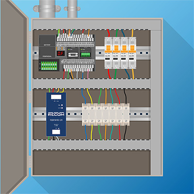 Fig. 1: Typical DIN rail installation
Advantages of the DIN Rail System
Fig. 1: Typical DIN rail installation
Advantages of the DIN Rail System
Firstly, the modular approach allows electrical cabinets and panels to be quickly assembled, moved, or rearranged for optimum use of the available space with only a standard electrician’s screwdriver as a tool. There is no drilling, cutting, or threading needed. Electrical cabinets and panels are often available with pre-installed rails so installation can begin immediately.
Secondly, the DIN rail system allows easy upgrading or repair without disrupting other components – a defective part can be simply unclipped and replaced without affecting the other components. If the new part happens to be slightly larger than the older module, then the existing components can be shifted along the rail to make space.
Thirdly, as the mounting rail dimensions are all standardized, parts from different manufacturers are interchangeable and mounting compatible. On a single rail, different electrical components can be freely mixed, so, for example, connector blocks can be placed next to power supplies to simplify the distribution of power and reduce the amount of cabling required, or actuator relays placed next to PLCs.
Fourthly, as you might expect from a German standard, the ease of mounting allows an organized, neat, and logical layout within the cabinet. This not only speeds up assembly by streamlining the whole construction process but simplifies maintenance and troubleshooting. All electrical contacts are accessible from the front without disconnecting any wiring and many electrical components have status or alarm indicators so that complex installations can be quickly inspected to find the fault.
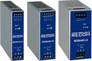 Fig. 2: REDIIN120, REDIIN240, and REDIIN480 DIN rail Power Supplies
Solutions include adding spacers between equipment to allow free air convection to cool the components, repositioning heat-generating components so that they are not in close proximity to one another, or, in extreme cases, adding fans to force-air cool the parts. The vertical separation between rails also needs to be considered so that warm air rising from one component does not adversely affect the component placed immediately above it. Fortunately, software packages are readily available that can be used to both plan the layout of the panel or cabinet in advance and to calculate the expected thermal loading. This software is often offered free by the cabinet manufacturers. More advanced software can also automatically check for compliance with electrical safety, construction, and technical standards, such as EN 61439.
RECOM is an established power supply manufacturer that is well-known for board-mounting or chassis-mounting embedded power, but also offers competitively priced AC/DC DIN rail mount power supplies (Figure 2).
Key Features of DIN Rail Power Supplies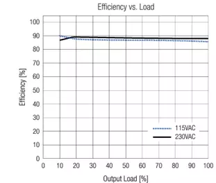 Fig. 3: Flat efficiency curve of the REDIIN120-24. No load power consumption is only 150mW
Design
Fig. 3: Flat efficiency curve of the REDIIN120-24. No load power consumption is only 150mW
Design
The products are fully certified according to international safety standards IEC/EN/UL 62368-1, IEC/EN/UL61010-1, and IEC/EN/UL/CSA61010-2-201. Electromagnetic radiated and conducted emissions are compliant with heavy industrial EN 61000-6-4 Class B Emission standard and EN 61000-6-2 Immunity standard.
The REDIIN series are designed for industrial, automation, power distribution, and test and measurement environments. These slim power supplies are ideal for applications in heavy engineering, production, home automation, data and telecom, traffic control, and water management—anywhere a compact, reliable, and cost-effective DC power supply is required within cabinets or electronic enclosures.
The post Slim DIN Rail Power Supplies For Industrial Applications appeared first on ELE Times.
The Software-Defined Vehicle Revolution: The Engineering Call to Action
The global automotive industry is undergoing its most profound transformation since the assembly line. This shift, driven by electrification and autonomy, is centrally powered by the Software-Defined Vehicle (SDV). For India’s vast pool of electronics and embedded systems engineers, this shift is more than just a trend—it’s a once-in-a-generation opportunity to become a global technology powerhouse in the automotive sector.
The stakes are enormous. India’s software-defined vehicle market is projected to witness a CAGR of 16.56% during the forecast period, FY2026-FY2033, growing from USD 2.69 billion in FY2025 to USD 9.16 billion in FY2033 through hardware, software, and subscription-based features. This piece breaks down the fundamental architectural shift, the commercial imperative driving it, and the precise skills Indian engineers must master to capture this monumental value.
The Architectural Flip: From Distributed Modules to Central Compute
For the last three decades, vehicle architecture was defined by a sprawling, distributed network of Electronic Control Units (ECUs). Modern cars can contain up to 150 dedicated ECUs, each dedicated to a narrow task (such as controlling a specific window or a part of the engine), which are scattered throughout the car.
Christopher Borroni-Bird, Founder of Afreecar, USA, notes, “The path to SDVs is a major disruption for automakers. It is a fundamental shift in value from hardware to software.”
The fundamental limitations of this legacy architecture are now a critical bottleneck for innovation:
- Complexity and Cost: This highly decentralized design requires kilometers of heavy, expensive wiring and complex communication protocols (like CAN and LIN), leading to massive complexity in integration and testing.
- Bandwidth Saturation: The low bandwidth of CAN limits the data throughput required by modern systems like Advanced Driver Assistance Systems (ADAS), which process gigabytes of sensor data per second.
- Inflexible Updates: Functionality is tied tightly to hardware, making it nearly impossible to introduce meaningful new features after the car leaves the factory.
The Software-Defined Vehicle solves this by replacing the distributed ECUs with a centralized, high-performance computing (HPC) approach. It consolidates functions into powerful, centrally or zonally placed compute units. This transformation moves through two key stages:
- Domain-Centralization (The Intermediate Step)
In the domain-centralized architecture, automakers consolidate dozens of small ECUs into a handful of powerful Domain Controllers—typically one each for powertrain, body, infotainment, and ADAS. These domain controllers are high-performance SoCs that replace clusters of ECUs within each functional region. While this significantly reduces ECU count and wiring complexity, it still maintains separation between critical domains. Engineers now need to handle thermal constraints, high-speed data movement, and virtualization middleware to ensure that safety-critical functions (like braking or steering) remain strictly isolated from non-critical ones (like media playback). This stage marks the shift from distributed electronics to consolidated compute, setting the foundation for full vehicle-centralized architectures.
- High-Speed Networking
High-speed networking is essential in SDVs because modern vehicles generate enormous volumes of data from cameras, radar, LiDAR, and other sensors—far beyond what the traditional CAN bus can carry. CAN was designed for millisecond-level control signals, not multi-megabit video streams or real-time sensor fusion. To solve this bottleneck, SDVs now use Automotive Ethernet as the central data backbone. It supports gigabit-level throughput and incorporates Time-Sensitive Networking (TSN) to ensure data is delivered with guaranteed timing, which is critical for ADAS decision-making.
In simple terms: Automotive Ethernet + TSN allows the car’s brain to receive huge amounts of sensor data quickly, predictably, and without delay—something CAN was never built for. This shift enables reliable perception, faster response times, and the scalable communication architecture required for autonomous and software-defined features.
The Commercial Imperative: Recurring Revenue and Lifetime Value
The architectural shift is driven equally by a dramatic change in the business model. Historically, an OEM’s revenue ceased the moment the car was sold. SDVs flip this model, transforming the vehicle into an evolving platform for recurring revenue. The technical architecture in SDVs is merely the enabling layer for an entirely new economic model. When a vehicle’s capabilities are defined by its software stack, the relationship with the customer becomes continuous.
The market potential for subscriptions, services, and features-on-demand is what drives the massive industry investment. Post-sale monetization opportunities include:
- Features-as-a-Service: Performance boosts, advanced ADAS capabilities, or heated seats activated temporarily via a subscription.
- Predictive Maintenance: Using vehicle data to predict failures, leading to service revenue and higher customer satisfaction.
- In-Car Commerce and Telematics: Partnerships for payment processing, insurance optimization, and fleet management services.
The Pillars of SDV Engineering: New Skill Requirements
To build the SDV, engineers must shift their focus from optimizing individual microcontrollers to designing entire systems based on high-performance computing, security, and real-time networking. The core skill pillars for the next generation of Indian automotive engineers are:
- High-Speed, Deterministic Networking
The shift from CAN/LIN (up to 1 Mbit/s) to Automotive Ethernet (100 Mbit/s to 10 Gbit/s) is essential to handle the massive data from LIDAR, radar, and HD cameras. Crucially, engineers must master Time-Sensitive Networking (TSN). TSN is the standard that guarantees deterministic data delivery—meaning a brake command always arrives in a precise, guaranteed timeframe, regardless of network traffic. This is a non-negotiable requirement for functional safety.
- Platform Virtualization and Mixed-Criticality Systems
The HPC runs software with varying safety requirements, known as mixed-criticality systems. A malfunction in the display stack must not crash the brake-by-wire system. This separation is achieved using two key technologies:
- Hypervisors (Type 1): Specialized hypervisors allow multiple operating systems (or execution environments) to run concurrently on the same HPC hardware, ensuring fault isolation and resource partitioning.
- Adaptive AUTOSAR: This next-generation middleware (replacing Classic AUTOSAR) is built to manage the complexity of centralized compute, supporting POSIX-compliant operating systems and service-oriented communication protocols necessary for dynamic, interconnected applications.
3. Functional Safety and Cybersecurity
With software controlling all critical systems, safety standards must be integrated at every layer of the architecture.
- ISO 26262 (Functional Safety): Engineers need proficiency in defining and implementing specific Automotive Safety Integrity Levels (ASIL) for every function. For example, ADAS features might require ASIL-D (the highest level).
- ISO/SAE 21434 (Cybersecurity): Connectivity exposes the vehicle to external threats. Expertise in Threat Analysis and Risk Assessment (TARA), secure boot, intrusion detection systems (IDS), and over-the-air (OTA) update security is mandatory to protect the vehicle throughout its 15-year lifecycle.
India’s Strategic Advantage and the Talent Gap
India is uniquely positioned to capitalize on this shift. The country already hosts the largest R&D and engineering centers outside of headquarters for nearly every global OEM and Tier-1 supplier (e.g., Bosch, Continental, Mercedes-Benz, Hyundai). Indian teams are already responsible for complex areas like Infotainment development, diagnostics, and component-level software.
However, a critical gap exists between foundational embedded skills and the advanced, systems-level expertise required for SDVs. The shortage is most acute in:
- System Architects: We need engineers who can define the holistic E/E architecture, not just code a single ECU. This requires an end-to-end view of hardware, software, networking, and safety protocols.
- High-Level Software (Full-Stack Automotive): Expertise in integrating cloud services (AWS, Azure) with the in-vehicle VOS, leveraging DevOps pipelines, and managing vast data streams for machine learning models running on the car’s edge processors.
- Low-Level Middleware and Safety: Deep competence in Adaptive AUTOSAR and hypervisor configuration, which allows the critical and non-critical software stacks to coexist safely.
The Call to Build
The SDV revolution demands that Indian engineers make a proactive pivot. The value chain is restructuring, and the future winners will be those who design the platforms, not just those who implement modules.
This transition requires investment—not just by multinational corporations, but by individual engineers and educational institutions. Universities must rapidly introduce a curriculum focused on high-speed communications (TSN), virtualization, and modern safety standards. Industry professionals must aggressively pursue certifications and hands-on experience in Adaptive AUTOSAR and HPC environments.
India has the talent base and the sheer numbers to become the world’s SDV hub. This opportunity is about moving up the value chain, leading innovation, and defining the future of mobility from Bengaluru, Pune, and Hyderabad. The vehicle is being redefined, and with the right strategy and swift action, Indian engineers can and must be the global architects of the Software-Defined Vehicle era.
The post The Software-Defined Vehicle Revolution: The Engineering Call to Action appeared first on ELE Times.
Big opportunity for India to fill the 700,000 worker shortage in the chip industry : IESA chief Ashok Chandak
Speaking at the CNBC-TV18 and Moneycontrol UP Tech Next Electronics and Semiconductor Summit on December 2 in Lucknow, president of the India Electronics and Semiconductor Association (IESA), Ashok Chandak stated that the global chip industry faces a deficit of 700,000 workers by 2030, and this can be used as a potential opportunity by India to fill the urgent gap.
Highlighting this opportunity, Chandak also threw light on the existing lack of skill training curriculum. For this he suggested a two-step model, updating technical curriculum to meet future needs and building manufacturing-related training programmes as India scales chip production.
He also added that IESA has already begun discussions with institutes on curriculum reform.
As the advancement in the industry continues to grow, the skill set required also needs to be updates and modified accordingly. The assimilation of Ai and machine learning with the use of technologies like digital twin and AR/VR have opened up the potential for the large Indian population of engineers and scientists to fulfil the demand as India strides ahead on its own India Semiconductor Mission (ISM), wherein the first ‘Made In India’ chip is expected to roll out by the end of December 2025.
The post Big opportunity for India to fill the 700,000 worker shortage in the chip industry : IESA chief Ashok Chandak appeared first on ELE Times.
Outages Won’t Wait: Why Grid Modernization Must Move Faster
Courtesy: Keysight Technologies
A routine click on a recommended link via the AI overview of my browser on November 18 yielded a glaring “internal server error” (Figure 1) when I clicked on a search-referenced website. The Cloudflare outage disrupted connectivity on various platforms, including ChatGPT, Canva, and X. Undaunted, the cyber community had a memes field day when services were restored, flooding their feeds with humorous outage memes.
 Fig1. Data center downtime can cause a host of end-user disruptions.
On a more serious note, data center and internet outages are no laughing matter, impacting businesses from online shopping to cryptocurrency exchanges. While the November outage at Cloudflare was attributed to configuration errors, another outage two years earlier was due to a power failure at one of its data centers in Oregon. Cloudflare is not alone in its outage woes. In fact, power failures outweigh network and IT issues when it comes to disrupting online user experiences.
Data from the 2025 Uptime Institute Global Data Center Survey shows that although 50% of data centers experienced at least one impactful outage over the past three years, down from 53% in 2024 (see Figure 2), power issues remain the top cause.
 Figure 2. Grid modernization is key to addressing power issues causing data center outages.
It’s not surprising that just a few years ago, electric vehicles (EVs) were deemed to be the new energy guzzlers of the decade, only to be rapidly overtaken by data centers. From crypto mining to generating “morph my cat to holiday mode” image creation prompts, each click adds strain to the power grid, not forgetting the heat generated.
 Figure 3. Meta AI’s response when asked how much energy it used to turn my homebody kitty into a cool cat on vacation.
Why must grid modernization happen sooner rather than later?
Data centers currently consume almost five times as much electricity as electric vehicles collectively, but both markets are expected to see a rise in demand for power in the coming years. In developed countries, power grids are already feeling the strain from these new energy guzzlers. Grid modernization must happen sooner rather than later to buffer the impact of skyrocketing electricity demand from both data centers and the EV market, to ensure the power grid’s resilience, stability, and security. Without swift upgrades, older grids are at risk of instability, outages, and bottlenecks as digital infrastructure and EV adoption accelerate.
What does grid modernization entail?
Grid modernization requires a strategic overhaul of legacy power infrastructure at the energy, communications, and operations levels, as illustrated in Figure 4. Existing energy infrastructure must be scalable and be able to incorporate and integrate renewable and distributed energy resources (DERs). Bi-directional communication protocols must continue to evolve to enable real-time data exchange between power-generating assets, energy storage systems, and end-user loads.
This transformation demands compliance with rigorous interoperability standards and cybersecurity frameworks to ensure seamless integration across heterogeneous systems, while safeguarding grid reliability and resilience against operational and environmental stresses.
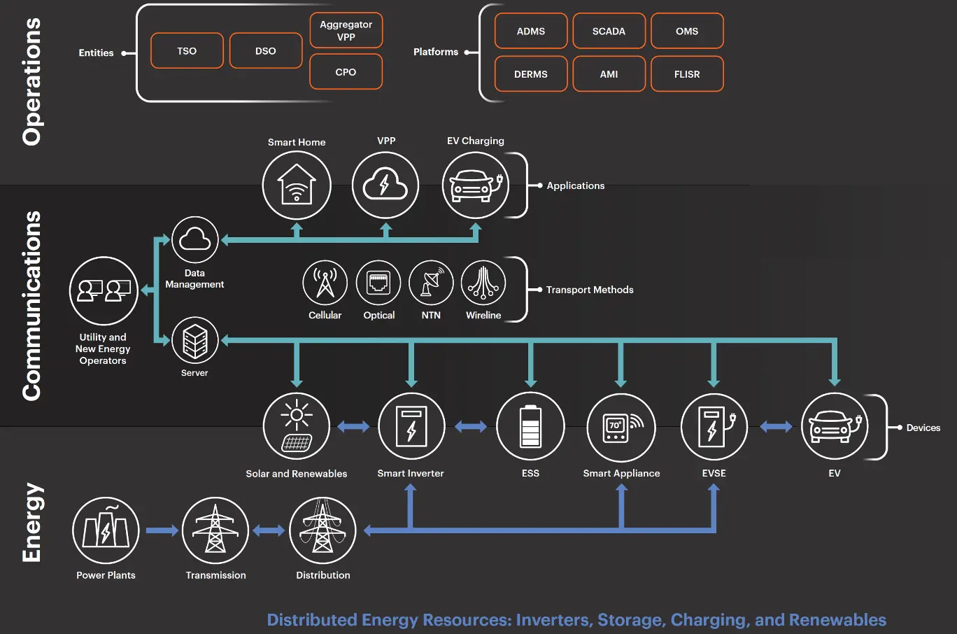 Figure 4. Grid modernization impacts a complex, interconnected energy ecosystem that must be thoroughly tested and validated to ensure grid reliability and resilience.
Towards Grid Resilience
Grid modernization can significantly reduce both data center outages and power shortages for EV charging, although the impact will depend on how fast the power infrastructure gets upgraded. The modernized grid will employ advanced sensors, automated controls, and predictive analytics to detect and isolate faults quickly. This will further reduce the number of data center outages due to power issues and mitigate the dips in power currently plaguing some cities’ EV charging infrastructure. As the world powers on with increasing load demands, our grid energy community must work together to plan, validate, and build a resilient grid.
Keysight can help you with your innovations for this exciting grid transformation. Our design validation and testing solutions cover inverter-based resources (IBRs) and distributed energy resources (DERs), to tools enabling systems integration and deployment, as well as operations.
The post Outages Won’t Wait: Why Grid Modernization Must Move Faster appeared first on ELE Times.
The Unsung Hero: How Power Electronics is Fueling the EV Charging Revolution
The electrifying shift towards Electric Vehicles (EVs) often dominates headlines—all talk of battery range, colossal Gigafactories, and the race to deploy charging stations. Yet, behind the spectacle of a simple “plug-in” lies an unheralded, decisive force: power electronics. Every single charging point, from a home unit to a highway beast, is fundamentally a high-voltage, high-efficiency energy conversion machine.
It is power electronics that determines the triad of performance critical to mass adoption: how efficiently, how safely, and how quickly energy moves from the grid into the vehicle’s battery. EV charging is not just about supplying electricity; it’s about converting, controlling, and conditioning power with near-perfect precision.
The Hidden Complexity of Converting Power
For the user, charging is seamless. For the engineer, the act of connecting a cable triggers a tightly choreographed sequence of power processing. An EV battery, which is DC-based, requires regulated DC power at a precise voltage and current profile. Since the public grid supplies AC (Alternating Current), a sophisticated conversion stage is mandatory. This conversion occurs in one of two places:
- Onboard Charger (OBC) for AC Charging: The charger station itself is simple, providing raw AC power. The vehicle’s OBC handles the conversion from AC to the regulated DC needed by the battery. The speed is thus limited by the OBC’s rating.
- DC Fast Charger (DCFC) for DC Charging: The station handles the entire conversion process, delivering high-power DC directly to the battery. This allows for speeds from 50kW up to 400kW or more, effectively eliminating range anxiety for long-distance travel.
Inside the Charger: The Power Stages
Further, let’s talk about the high-power DCFC, where power electronics is the key protagonist, executing a meticulous multi-stage architecture:
- AC-DC Power Factor Correction (PFC) Stage: Incoming AC from the three-phase grid is first rectified into DC. Crucially, active PFC circuits shape the input current waveform to be purely sinusoidal and in phase with the voltage. This is not just for efficiency; it is essential for grid stability, ensuring low Total Harmonic Distortion (THD) and preventing adverse effects on other loads connected to the same grid segment. This stage establishes a stable DC link voltage.
- DC-DC High-Frequency Conversion Stage: This is the heart of the fast charger. A high-frequency, isolated converter takes the DC link voltage and steps it up or down to precisely match the varying voltage requirements of the EV battery (which changes dynamically during the charging cycle). Topologies like the Phase-Shift Full Bridge (PSFB) or the Dual Active Bridge (DAB) converter are chosen for their ability to handle high power, achieve high efficiency, and, in the case of DAB, support bidirectional power flow.
- Output Filtering and Control: The final DC output passes through filters to remove ripple. Real-time digital controllers—often high-speed Digital Signal Processors (DSPs)—continuously monitor the battery’s voltage, current, and temperature, adjusting the DC-DC stage’s switching duty cycle every microsecond to adhere strictly to the battery’s requested charging profile.
The SiC-GaN Turning Point
The revolution in charging speed, size, and efficiency is inseparable from the emergence of Wide Bandgap (WBG) Semiconductors: Silicon Carbide (SiC) and Gallium Nitride (GaN). These materials possess a wider energy bandgap than traditional silicon, enabling them to operate at higher voltages, higher temperatures, and significantly higher switching frequencies. Let’s understand how these make EV charging an easier game.
- SiC in High-Power Chargers: SiC MOSFETs have become the industry standard for fast chargers in the 30kW-350 kW range. They boast a breakdown voltage up to 1700V and substantially lower switching losses compared to silicon IGBTs or MOSFETs. This is critical because reduced losses mean less energy wasted as heat, which translates to:
- Higher System Efficiency: Reducing the operational cost for the charging network operator.
- Reduced Cooling Requirements: Simplifying the thermal management system, a crucial factor in India’s high ambient temperatures.
- Smaller Component Size: Operating at higher frequencies allows for smaller, lighter passive components (like inductors and transformers), leading to denser, more compact charging cabinets.
- GaN in High-Frequency Systems: GaN devices excel in extremely high-frequency switching, often used in auxiliary power supplies, high-density AC-DC stages, and compact onboard chargers. Their extremely low gate charge and fast switching characteristics allow for even lighter magnetics and smaller overall designs than SiC, pushing the boundaries of power density.
The combined adoption of SiC for the main power stages and GaN for high-frequency auxiliary and lower-power segments represents the current state-of-the-art in charging technology design.
Smart Power: Digital Control and Bidirectionality
A modern EV charger is far more than a simple power converter; it is a complex, intelligent electronic system. The digital controllers (DSPs and microcontrollers) not only manage the power stages but also the critical communications and safety protocols.
Embedded Control Systems
These control systems operate with microsecond-level precision, handling the generation of Pulse Width Modulation (PWM) signals for the power switches, monitoring multiple feedback loops (voltage, current, temperature), and executing complex thermal management algorithms. They are the guardians of safety, instantly detecting and shutting down fault events like overcurrent or ground faults.
Grid and Vehicle Communication
The intelligence extends to multiple layers of communication, ensuring seamless integration with the vehicle and the backend network:
- OCPP (Open Charge Point Protocol): Used to communicate with the central management system (CMS) for remote monitoring, status updates, user authentication, and billing.
- ISO 15118: A crucial standard for secure Plug-and-Charge functionality, allowing the vehicle and charger to negotiate power delivery and payment automatically.
- PLC/CAN: The communication protocols used for the real-time Battery Management System (BMS) handshake, which dictates the exact power level the battery can safely accept at any given moment.
This digital brain is paving the way for the next critical frontier: bidirectional charging, or Vehicle-to-Grid (V2G).
The Policy Framework and India’s Drive for Localization
India’s aggressive push for electric mobility is backed by a robust, multi-layered policy structure designed to address both the demand and the infrastructure challenge, propelling the local power electronics ecosystem.
The recently notified PM E-DRIVE (Electric Drive Revolution in Innovative Vehicle Enhancement) Scheme, succeeding FAME-II, underscores the government’s commitment, with an outlay of ₹10,900 crore. Crucially, a significant portion of this fund is earmarked for EV Public Charging Stations (EVPCS).
Key Infrastructure Incentives:
- PM E-DRIVE Incentives: This scheme offers substantial financial support for deploying charging infrastructure, with a specific focus on setting up a widespread network. The Ministry of Heavy Industries (MHI) has offered incentives for states to secure land, build upstream infrastructure (transformers, cables), and manage the rollout, bearing up to 80% of the upstream infrastructure cost in some cases.
- Mandated Density: The EV Charging Infrastructure Policy 2025 sets clear mandates for density—aiming for a charging station every 3 km X 3 km grid in cities and every 25 km on both sides of highways.
- Tariff Rationalization: The Ministry of Power has moved to ensure that the tariff for the supply of electricity to public EV charging stations is a single-part tariff and remains affordable, aiding the business case for operators.
- Building Bylaw Amendments: Model Building Bye-Laws have been amended to mandate the inclusion of charging stations in private and commercial buildings, pushing for destination charging and easing urban range anxiety.
Focus on Localization and Self-Reliance:
A critical mandate across all policies, including PM E-DRIVE and the broader Production Linked Incentive (PLI) Scheme for Advanced Chemistry Cell (ACC) Battery Storage and Automotive Components, is localization. The MHI insists that all incentivized chargers comply with the Phased Manufacturing Programme (PMP), demanding an increasing percentage of domestic value addition in components like charging guns, software, controllers, and power electronic modules.
This push is creating a substantial market for Indian engineers to develop:
- Custom SiC-based fast-charger modules.
- Thermal management and enclosure designs optimized for Indian operating conditions (dust, heat, humidity).
- Indigenous control algorithms and communication protocols.
The convergence of supportive policy and cutting-edge power electronics technology is making India a central stage for the global evolution of charging infrastructure. The country’s engineers are not just deploying technology; they are actively shaping it to meet a unique and demanding environment.
The success of electric mobility is a story often told about batteries and cars, but it is fundamentally a story about energy conversion. EV charging is not merely an electrical transition; it is a power electronics revolution. The engineers building these advanced, intelligent power systems are the true architects defining the future of transport.
The post The Unsung Hero: How Power Electronics is Fueling the EV Charging Revolution appeared first on ELE Times.
Emerging Technology Trends in EV Motors
Electric Vehicles (EVs), central to the global climate transition, are also becoming crucial drivers of engineering innovation. At the heart of this transformation lies the electric motor, an area now attracting intense R&D focus as automakers chase higher efficiency, lower material dependency, and superior driving performance.
Conventional Motor Choices: IM, PMSM, and BLDC
Most EVs today rely on three key motor architectures:
– Induction Motors (IM): Rugged but less efficient.
– Permanent Magnet Synchronous Motors (PMSM): Highly efficient and used in high-performance vehicles.
– Brushless DC Motors (BLDC): Lightweight and ideal for scooters and bikes, using electronic commutation instead of brushes.
While these motors have served well, next-generation EV demands—compact packaging, higher power density, optimized cooling, and smarter control—are pushing the industry toward more advanced technologies.
What’s Driving the Next Wave of Motor Innovation
Manufacturers today are actively pursuing:
– Reduction in installation space
– Higher power-to-weight ratios
– Improved thermal management
– Lower reliance on rare-earth materials
– Greater efficiency through refined control electronics
These needs are shaping emerging motor technologies that promise major shifts in EV design.
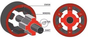
Axial Flux Motors: Compact Powerhouses of the FutureAxial flux motors—often called “pancake motors”—use disc-shaped stators and rotors. Unlike traditional radial flux machines, their magnetic field flows parallel to the shaft.
Key strengths:
– Extremely compact
– Exceptionally high power density
– Ideal for performance-focused EVs
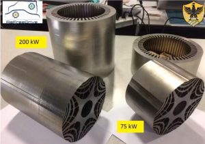
A standout example is YASA, a Mercedes-owned company whose prototype axial flux motor delivers 550 kW (737 hp) at just 13.1 kg, achieving a record 42 kW/kg specific power.
Key challenge: Maintaining a uniform air gap is difficult due to strong magnetic attraction, making heat dissipation more demanding.
 Switch Reluctance Motors (SRM): Simple, Strong, Magnet-Free
Switch reluctance motors operate using reluctance torque, relying solely on magnetic attraction rather than electromagnetic induction or permanent magnets. The rotor contains no windings or magnets, significantly reducing rare-earth dependence.
Advantages:
– Robust and simple construction
– Low material cost
– High torque potential
Companies like Enedym, Turnitude Technologies, and Advanced Electric Machines (AEM) are actively advancing SRM technology.
Challenges:
– High torque ripple
– Noise and vibration
– More complex control electronics due to trapezoidal DC waveforms
Increasing the number of stator/rotor teeth can reduce ripple but adds manufacturing complexity.
 Synchronous Reluctance Motors (SynRM): Tackling Torque Ripple
SynRMs were developed to overcome the noise and vibration issues of SRMs. Their rotor design uses multiple layered air gaps, creating a shaped flux path that enhances torque production.
Key benefits:
– Operates on sinusoidal waveforms
– Much lower torque ripple
– No magnets required
– Improved noise characteristics
A well-known adaptation is seen in the Tesla Model 3, which uses a SynRM with internal segmented permanent magnets to reduce eddy-current losses and thermal buildup.
 In-Wheel Motors: Reinventing Torque Delivery at the Wheels
In-wheel motor technology places a dedicated motor inside each wheel, eliminating conventional drivetrains.
Advantages:
– Increased interior space
– Reduced transmission losses
– Precise torque vectoring for improved handling
– Lower mechanical maintenance
GEM Motors, a Slovenian startup, has developed compact, modular in-wheel motor systems that claim up to 20% increased driving range without additional battery capacity.
Challenge:
In-wheel placement increases unsprung mass, affecting ride quality and requiring highly compact yet high-torque designs.
 The Road Ahead: Designing Motors for a Resource-Constrained Future
With rising pressure on rare-earth supply chains and the push for higher efficiency, the next generation of EV motors must strike a balance between performance, sustainability, manufacturability, and cost. Technologies minimizing rare-earth usage, improving thermal robustness, and reducing weight will define the industry’s trajectory. As innovation accelerates, electric motors will not just power vehicles—they will shape the future of clean, intelligent, and resource-efficient mobility.
The post Emerging Technology Trends in EV Motors appeared first on ELE Times.
Terahertz Electronics for 6G & Imaging: A Technical Chronicle
As the demand for more spectrum increased with the extensive usage of mobile data, XR/VR, sensing, and autonomous systems, the sub-THz region (100–300 GHz and beyond) emerges as a compelling frontier. In effect, we are approaching the limits of what mm Wave alone can deliver at scale. The THz band promises immense contiguous spectrum, enabling links well above 100 Gbps, and the possibility of co-designing communication and high-resolution sensing (imaging/radar) in a unified platform.
Yet this promise confronts severe physical obstacles: high path loss, molecular absorption, component limitations, packaging losses, and system complexity. This article traces how the industry is navigating those obstacles, what is working now, what remains open, and where the first real systems might land.
The Early Milestones: Lab Prototypes That MatterA landmark announcement came in October 2024 from NTT: a compact InP-HEMT front-end (FE) that achieved 160 Gbps in the 300 GHz band by integrating mixers, PAs, LNAs, and LO PAs in a single IC.
Key technical innovations in that work include:
- A fully differential configuration to cancel local-oscillator (LO) leakage, critical at THz frequencies.
- Reduction of module interconnections (thus insertion loss) by integrating discrete functions into a monolithic chip.
- Shrinking module size from ~15 cm to ~2.8 cm, improving form factor while widening operational bandwidth.
More recently, in mid-2025, NTT (with Keysight and its subsidiary NTT Innovative Devices) demonstrated a power amplifier module capable of 280 Gbps (35 GBaud, 256-QAM) in the J-band (≈220–325 GHz), albeit at 0 dBm output power. This points toward simultaneous scaling of both bandwidth and linear output power, a crucial step forward.
On the standardization/architectural front, partnership experiments like Keysight + Ericsson’s “pre-6G” prototype show how new waveforms and stacks might evolve. In 2024, they demonstrated a base station + UE link (modified 5G stack) over new frequency bands, signaling industry interest in evolving existing layers to support extreme throughput. Ericsson itself emphasizes that 6G will mix evolved and new concepts spectrum aggregation, ISAC, spatial awareness, and energy-efficient designs.
These milestones are not “toy results” they validate that the critical component blocks can already support high-throughput, multi-GHz signals, albeit in controlled lab settings.
Technical Foundations: Devices, Architectures, and PackagingTo move from prototypes to systems, several technical foundations must be matured in parallel:
Device and Front-End Technologies- InP / III–V HEMTs and HBTs remain leading candidates for mixers, LNAs, and PAs at high frequencies, thanks to superior electron mobility and gain.
- SiGe BiCMOS bridges the gap, often handling LO generation, control logic, and lower-frequency blocks, while III–V handles the toughest RF segments.
- Schottky diodes, resonant tunneling diodes (RTDs), and nonlinear mixers play roles for frequency translation and LO generation.
- Photonic sources such as UTC photodiodes or photomixing supplement generation in narrowband, coherent applications. For example, a modified uni-traveling-carrier photodiode (MUTC-PD) has been proposed for 160 Gbps over D-band in a fiber-THz hybrid link.
The challenge is achieving sufficient output power, flat gain over multi-GHz bandwidth, linearity, and noise performance, all within thermal and size constraints.
Architectures and Signal Processing- Multiplication chains (cascaded frequency multipliers) remain the standard path for elevating microwave frequencies into THz.
- Harmonic or sub-harmonic mixing eases LO generation but while managing phase noise is critical.
- Beamforming / phased arrays are essential. Directive beams offer path-loss mitigation and interference control. True-time delay or phase shifting (with very fine resolution) is a design hurdle at THz.
- Waveforms must tolerate impairments (phase noise, CFO). Hybrid schemes combining single-carrier plus OFDM and FMCW / chirp waveforms are under study.
- Joint sensing-communication (ISAC): Using the same waveform for data and radar-like imaging is central to future designs.
- Channel modeling, beam training, blockage prediction, and adaptive modulation are crucial companion software domains.
At THz, packaging and interconnect losses can kill performance faster than device limitations.
- Antenna-in-package (AiP) and antenna-on-substrate (e.g. silicon lens, meta surfaces, dielectric lens) help reduce the distance from active devices to radiating aperture.
- Substrate-integrated waveguides (SIW), micromachined waveguides, quasi-optical coupling replace lossy microstrip lines and CPWs.
- Thermal spreaders, heat conduction, and material selection (low-loss dielectrics) are critical for sustaining device stability.
- Calibration and measurement: On-wafer TRL/LRM up to sub-THz, over-the-air (OTA) test setups, and real-time calibration loops are required for production test.
Propagation in THz is unforgiving:
- Free-space path loss (FSPL) scales with frequency. Every additional decade in frequency adds ~20 dB loss.
- Molecular absorption, especially from water vapor, introduces frequency-specific attenuation notches; engineers must choose spectral windows (D-band, G-band, J-band, etc.).
- Blockage: Humans, objects, and materials often act as near-total blockers at THz.
- Multipath is limited — channels tend toward sparse tap-delay profiles.
Thus, THz is suited for controlled, short-range, high-throughput links or co-located sensing+ communication. Outdoor macro coverage is generally impractical unless beams are extremely narrow and paths well managed. Backhaul and hotspot links are more feasible use cases than full wide-area coverage.
Imaging and Sensing Use CasesUnlike pure communication, imaging demands high dynamic range, spatial resolution, and sometimes passive operation. THz enables:
- Active coherent imaging (FMCW, pulsed radar) for 3D reconstruction, industrial NDT, and package inspection.
- Passive imaging / thermography for detecting emissivity contrasts.
- Computational imaging via coded apertures, compressed sensing, and meta surface masks to reduce sensor complexity.
In system designs, the same front-end and beam infrastructure may handle both data and imaging tasks, subject to power and SNR trade-offs.
Roadmap & Open ProblemsWhile lab successes validate feasibility, many gaps remain before field-ready systems:
- Watt-class, efficient THz sources at room temperature (particularly beyond 200 GHz).
- Low-loss, scalable passives and interconnects (waveguide, delay lines) at THz frequencies.
- Robust channel models across environments (indoor, outdoor, humidity, mobility) with validation data.
- Low-cost calibration / test methodologies for mass production.
- Integrated ISAC signal processing and software stacks that abstract complexity from system integrators.
- Security and coexistence in pencil-beam, high-frequency environments.
The next decade will see THz systems not replacing, but supplementing existing networks. They will begin in enterprise, industrial, and hotspot contexts (e.g. 100+ Gbps indoor links, wireless backhaul, imaging tools in factories). Over time, integrated sensing + communication systems (robotics, AR, digital twins) will leverage THz’s ability to see and talk in the same hardware.
The core enablers: heterogeneous integration (III-V + CMOS/BiCMOS), advanced packaging and optics, robust beamforming, and tightly coupled signal processing. Lab records such as 160 Gbps in the 300 GHz front-end by NTT, and 280 Gbps in a J-band PA module show that neither bandwidth nor throughput is purely theoretical — the next steps are scaling power, cost, and reliability.
The post Terahertz Electronics for 6G & Imaging: A Technical Chronicle appeared first on ELE Times.
When Tiny Devices Get Big Brains: The Era of Edge and Neuromorphic AI
From data-center dreams to intelligence at the metal
Five years ago “AI” largely meant giant models running in faraway data centers. However, today the story is different, where intelligence is migrating to the device itself, in phones, drones, health wearable’s, factory sensors. This shift is not merely cosmetic, instead it forces the hardware designers to ask: how do you give a tiny, thermally constrained device meaningful perception and decision-making power? As Qualcomm’s leadership puts it, the industry is “in a catbird seat for the edge AI shift,” and the battle is now about bringing capable, power-efficient AI onto the device.
Why edge matters practical constraints, human consequences
There are three blunt facts that drive this migration: latency (milliseconds matter for robots and vehicles), bandwidth (you can’t stream everything from billions of sensors), and privacy (health or industrial data often can’t be shipped to the cloud). The combination changes priorities: instead of raw throughput for training, the trophy is energy per inference and predictable real-time behavior.
How the hardware world is responding
Hardware paths diverge into pragmatic, proven accelerators and more speculative, brain-inspired designs.
- Pragmatic accelerators: TPUs, NPUs, heterogeneous SoCs.
Google’s Edge TPU family and Coral modules demonstrate the pragmatic approach: small, task-tuned silicon that runs quantized CNNs and vision models with tiny power budgets. At the cloud level Google’s new TPU generations (and an emerging Ironwood lineup) show the company’s ongoing bet on custom AI silicon spanning cloud to edge. - Mobile/SoC players double down: Qualcomm and others are reworking mobile chips for on-device AI, shifting CPU micro architectures and embedding NPUs to deliver generative and perception workloads in phones and embedded devices. Qualcomm’s public positioning and product roadmaps are explicit: the company expects edge AI to reshape how devices are designed and monetized.
- In-memory and analog compute: to beat the von Neumann cost of moving data. Emerging modules and research prototypes put compute inside memory arrays (ReRAM/PCM) to slash energy per operation, an attractive direction for always-on sensing.
The wild card: neuromorphic computing
If conventional accelerators are an evolutionary path, neuromorphic chips are a more radical reimagination. Instead of dense matrix math and clocked pipelines, neuromorphic hardware uses event-driven spikes, co-located memory and compute, and parallel sparse operations — the same tricks biology uses to run a brain on ~20 W.
Intel, one of the earliest movers, says the approach scales: Loihi research chips and larger systems (e.g., the Hala Point neuromorphic system) show how neuromorphic designs can reach hundreds of millions or billions of neurons while keeping power orders of magnitude lower than conventional accelerators for certain tasks. Those investments signal serious industrial interest, not just academic curiosity.
Voices from the field: what leaders are actually saying
- “We’re positioning for on-device intelligence not just as a marketing line, but as an architecture shift,” paraphrase of Qualcomm leadership describing the company’s edge AI strategy and roadmap.
- “Neuromorphic systems let us explore ultra-low power, event-driven processing that’s ideal for sensors and adaptive control,” Intel’s Loihi programme commentary on the promise of on-chip learning and energy efficiency.
- A recent industry angle: big platform moves (e.g., companies making development boards and tighter dev ecosystems available) reflect a desire to lower barriers. The Qualcomm–Arduino alignment and new low-cost boards aim to democratize edge AI prototyping for millions of developers.
Where hybrid architecture wins: pragmatic use cases
Rather than “neuromorphic replaces everything,” the likely near-term scenario is hybrid systems:
- Dense pretrained CNNs (object detection, segmentation) run on NPUs/TPUs.
- Spiking neuromorphic co-processors handle always-on tasks: anomaly detection, low-latency sensor fusion, prosthetic feedback loops.
- Emerging in-memory modules reduce the energy cost of massive matrix multiplies where appropriate.
Practical example: an autonomous drone might use a CNN accelerator for scene understanding while a neuromorphic path handles collision avoidance from event cameras with microsecond reaction time.
Barriers: the messy middle between lab and product
- Algorithmic mismatch: mainstream ML is dominated by backpropagation and dense tensors; mapping these workloads efficiently to spikes or in-memory analog is still an active research problem.
- Tooling and developer experience: frameworks like PyTorch/TensorFlow are not native to SNNs; toolchains such as Intel’s Lava and domain projects exist but must mature for broad adoption.
- Manufacturing & integration: moving prototypes into volume production and integrating neuromorphic blocks into SoCs poses yield and ecosystem challenges.
Market dynamics & the investment climate
There’s heavy capital flowing into edge AI and neuromorphic startups, and forecasts project notable growth in neuromorphic market value over the coming decade. That influx is tempered by a broader market caution — public leaders have noted hype cycles in AI investing but history shows that even bubble phases can accelerate technological foundations that persist.
Practical advice for engineering and product teams
- Experiment now prototype with Edge TPUs/NPUs and cheap dev boards (Arduino + Snapdragon/Dragonwing examples are democratizing access) to validate latency and privacy requirements.
- Start hybrid design thinking split workloads into dense inference (accelerator) vs event-driven (neuromorphic) buckets and architect the data pipeline accordingly.
- Invest in tooling and skill transfer train teams on spiking networks, event cameras, and in-memory accelerators, and contribute to open frameworks to lower porting costs.
- Follow system co-design unify hardware, firmware, and model teams early; the edge is unforgiving of mismatches between model assumptions and hardware constraints.
Conclusion: what will actually happen
Expect incremental but practical wins first: more powerful, efficient NPUs and smarter SoCs bringing generative and perception models to phones and industrial gateways. Parallel to that, neuromorphic systems will move from research novelties into niche, high-value roles (always-on sensing, adaptive prosthetics, extreme low-power autonomy).
The real competitive winners will be organizations that build the whole stack: silicon, software toolchains, developer ecosystems, and use-case partnerships. In short: intelligence will increasingly live at the edge, and the fastest adopters will design for hybrid, energy-aware systems where neuromorphic and conventional accelerators complement not replace each other.
The post When Tiny Devices Get Big Brains: The Era of Edge and Neuromorphic AI appeared first on ELE Times.
Inside the Hardware Lab: How Modern Electronic Devices Are Engineered
The engineering of contemporary electronic devices reflects a convergence of system thinking, material maturity, multidisciplinary collaboration, and accelerated development cycles. In laboratories across the world, each new product emerges from a structured, iterative workflow that integrates architecture, hardware, firmware, testing, and manufacturing considerations into a cohesive design process. As electronic systems become more compact, intelligent, and operationally demanding, the pathway from concept to certified production device requires a high level of methodological discipline.
This article outlines how modern electronics are engineered, focusing on workflows, design considerations, and the interdependencies that define professional hardware development today.
Requirements Engineering: Establishing the Foundation
The design of any electronic device begins with a comprehensive articulation of requirements. These requirements typically combine functional objectives, performance targets, environmental constraints, safety expectations, and compliance obligations.
Functional objectives determine what the system must achieve, whether sensing, processing, communication, actuation, or power conversion. Performance parameters such as accuracy, latency, bandwidth, power consumption, and operating lifetime define the measurable boundaries of the design. Environmental expectations—temperature range, ingress protection, shock and vibration tolerance, electromagnetic exposure, and mechanical stresses—shape the system’s robustness profile.
Regulatory frameworks, including standards such as IEC, UL, BIS, FCC, CE, and sector-specific certifications (automotive, medical, aerospace), contribute additional constraints. The initial requirement set forms the reference against which all subsequent design decisions are evaluated, creating traceability between intent and implementation.
System Architecture: Translating Requirements into Structure
System architecture bridges conceptual requirements and concrete engineering design. The process involves defining functional blocks and selecting computational, sensing, power, and communication strategies capable of fulfilling the previously established criteria.
The architecture phase typically identifies the processing platform—ranging from microcontrollers to SoCs, MPUs, or FPGAs—based on computational load, determinism, power availability, and peripheral integration. Communication subsystems are established at this stage, covering interfaces such as I²C, SPI, UART, USB, CAN, Ethernet, or wireless protocols.
The power architecture also takes shape here, mapping energy sources, conversion stages, regulation mechanisms, and protection pathways. Considerations such as thermal distribution, signal isolation, noise-sensitive regions, and preliminary enclosure constraints influence the structural arrangement. The architectural framework becomes the guiding reference for schematic and PCB development.
Component Selection: Balancing Performance, Reliability, and Lifecycle
Modern device design is deeply influenced by semiconductor availability, lifecycle predictability, and performance consistency. Component selection involves more than identifying electrically suitable parts; it requires an understanding of long-term supply chain stability, tolerance behaviour, temperature performance, reliability data, and compatibility with manufacturing processes.
Processors, sensors, regulators, discrete, passives, communication modules, and protection components are evaluated not only for electrical characteristics but also for de-rating behaviours, thermal performance, and package-level constraints. Temperature coefficients, impedance profiles, safe-operating-area characteristics, clock stability, and signal integrity parameters become central evaluation factors.
The resulting bill of materials represents an intersection of engineering decisions and procurement realities, ensuring the device can be produced reliably throughout its intended lifespan.
Schematic Design: The Logical Core of the Device
Schematic design formalizes the architectural plan into detailed electrical connectivity. This stage defines logical relationships, reference paths, power distribution, signal conditioning, timing sequences, and safety structures.
Circuit blocks—analog conditioning, digital logic, power conversion, RF front-ends, sensor interfaces, and display or communication elements—are designed with full consideration of parasitic behaviour, noise propagation, and functional dependencies. Power distribution requires careful sequencing, decoupling strategies, transient response consideration, and ripple management. Signal interfaces require appropriate level shifting, impedance alignment, and termination strategies.
Test points, programming headers, measurement references, and diagnostic interfaces are defined at this stage to ensure observability during validation. The schematic ultimately serves as the authoritative source for layout and firmware integration.
PCB Layout: Integrating Electrical, Mechanical, and Thermal Realities
PCB layout transforms the schematic into a physical system where electrical performance, manufacturability, and thermal behaviour converge. The arrangement of components, routing topology, layer stack-up, ground referencing, and shielding determines the system’s electromagnetic and thermal characteristics.
High-speed interfaces require controlled impedance routing, differential pair tuning, length matching, and clear return paths. Power networks demand minimized loop areas, appropriate copper thickness, and distribution paths that maintain voltage stability under load. Sensitive analog signals are routed away from high-noise digital or switching-power regions. Thermal dissipation—achieved through copper pours, thermal vias, and heat-spreading strategies—ensures the system can sustain continuous operation.
Mechanical constraints, such as enclosure geometry, connector placement, mounting-hole patterns, and assembly tolerances, influence layout decisions. The PCB thus becomes a synthesized embodiment of electrical intent and mechanical feasibility.
Prototyping and Hardware Bring-Up: Validating the Physical Implementation
Once fabricated, the prototype enters hardware bring-up, a methodical verification process in which the design is examined against its expected behavior. Validation typically begins with continuity and power integrity checks, ensuring that supply rails meet voltage, ripple, and transient requirements.
System initialization follows, involving processor boot-up, peripheral activation, clock stability verification, and interface-level communication checks. Subsystems are evaluated individually—power domains, sensor blocks, RF modules, analog interfaces, digital buses, and storage components.
Observations from oscilloscopes, logic analyzers, current probes, and thermal imagers contribute to a detailed understanding of the device’s operational profile. Any deviations from expected behavior guide iterative optimization in subsequent revisions.
Firmware Integration: Achieving Functional Cohesion
Firmware integration establishes coordination between hardware capabilities and system functionality. Board-support packages, peripheral drivers, middleware stacks, and application logic are aligned with the hardware’s timing, power, and performance characteristics.
Real-time constraints influence the choice of scheduling structures—whether bare-metal loops, cooperative architectures, or real-time operating systems. Communication stacks, sensor acquisition pipelines, memory management, and power-state transitions are implemented and tested on the physical hardware.
Interaction between firmware and hardware exposes edge cases in timing, voltage stability, electromagnetic sensitivity, or analog behavior, which often inform refinements in both domains.
Validation and Testing: Confirming Performance, Robustness, and Compliance
Comprehensive testing examines a device’s functionality under nominal and boundary conditions. Functional validation assesses sensing accuracy, communication stability, user-interface behavior, control logic execution, and subsystem interoperability. Reliability evaluation includes thermal cycling, vibration exposure, mechanical stress tests, humidity conditioning, and operational aging.
Electromagnetic compatibility testing examines emissions and immunity, including radiated and conducted profiles, ESD susceptibility, fast transients, and surge resilience. Pre-compliance evaluation during early prototypes reduces the probability of redesign during final certification stages.
Data collected during validation ensures that the system behaves predictably throughout its expected operating envelope.
Manufacturing Readiness: Transitioning from Prototype to Production
Production readiness involves synchronizing design intent with assembly processes, quality frameworks, and cost structures. Design-for-manufacturing and design-for-assembly considerations ensure that the device can be fabricated consistently across multiple production cycles.
Manufacturing documentation—including fabrication drawings, Gerber files, pick-and-place data, test specifications, and assembly notes—forms the reference package for contract manufacturers. Automated test equipment, in-circuit test fixtures, and functional test jigs are developed to verify each assembled unit.
Bill-of-materials optimization, yield analysis, and component sourcing strategies ensure long-term production stability.
Compliance and Certification: Meeting Regulatory Obligations
Final certification ensures that the device adheres to the safety, electromagnetic, and environmental requirements of the markets in which it will be deployed. Testing laboratories evaluate the system against regulatory standards, verifying electrical safety, electromagnetic behaviour, environmental resilience, and user-level protections.
The certification phase formalizes the device’s readiness for commercial deployment, requiring complete technical documentation, traceability data, and repeatable test results.
Lifecycle Management: Sustaining the Design Beyond Release
After the product reaches the market, lifecycle management ensures its sustained usability and manufacturability. Engineering change processes address component obsolescence, firmware enhancements, mechanical refinements, or field-observed anomalies.
Long-term reliability data, manufacturing feedback, and supplier updates contribute to ongoing revisions. In connected systems, firmware updates may be deployed over the air, extending functionality and addressing vulnerabilities.
Lifecycle management closes the loop between deployment and continuous improvement.
Conclusion
The design of a modern electronic device is a coordinated engineering endeavour that integrates requirements analysis, architectural planning, hardware design, firmware development, validation, manufacturing readiness, and lifecycle stewardship. Each stage influences the next, forming a continuous chain of interdependent decisions.
As technological expectations expand, the engineering methodologies supporting electronic design continue to mature. The result is a disciplined, multi-phase workflow that enables the creation of devices that are reliable, certifiable, scalable, and aligned with the complex operational demands of contemporary applications.
The post Inside the Hardware Lab: How Modern Electronic Devices Are Engineered appeared first on ELE Times.
EDOM Seminar Explores the Next Generation of Physical AI Robots Powered by NVIDIA Jetson Thor
The wave of innovation driven by generative AI is sweeping the globe, and AI’s capabilities are gradually extending from language understanding and visual recognition to action intelligence closer to real-world applications. This change makes physical AI, which integrates “perception, reasoning, and action,” the next important threshold for robotics and smart manufacturing. To help Taiwanese industries grasp this multimodal trend, EDOM Technology will hold the “AI ×Multimodal Robotics: New Era of Industrial Intelligence Seminar” on December 3, showcasing NVIDIA Jetson Thor, the ultimate platform for physical AI and robotics, and featuring insights from ecosystem partners who will share innovative applications spanning smart manufacturing, autonomous machines, and education.
As AI technology rapidly advances, robotics is shifting from the traditional perception and response model to a new stage where they can autonomously understand and participate in complex tasks. The rise of multimodal AI enables machines to simultaneously integrate image, voice, semantic, and spatial information, making more precise judgments and actions in the real world, making it possible to “know what to do” and “know how to do it.” As AI capabilities extend from the purely digital realm to the real world, physical AI has become a core driving force for industrial upgrading.
Multimodal × Physical AI: The Next Key Turning Point in Robotics
The seminar focuses on the theme of “Physical AI Driving the Intelligent Revolution of Robotics”, explores how AI, through multimodal perception and autonomous action capabilities, is reshaping the technical architecture and application scenarios of human-machine collaboration. Through technical sharing and case analysis, the seminar will help companies grasp the next turning points of smart manufacturing.
This event will focus on NVIDIA Jetson Thor and its software ecosystem, providing a panoramic view of future-oriented multimodal robotics technology. The NVIDIA Jetson Thor platform combines high-performance GPUs, edge computing, and multimodal understanding to complete perception, inference, decision-making, and action planning all at the device level, significantly improving robot autonomy and real-time responsiveness. Simultaneously, the platform is deeply integrated with NVIDIA Isaac, NVIDIA Metropolis, and NVIDIA Holoscan, creating an integrated development environment from simulation, verification, and testing to deployment, thus accelerating the implementation of intelligent robots and edge AI solutions. NVIDIA Jetson Thor also supports LLM, visual language models (VLMs), and various generative AI models, enabling machines to interpret their surroundings, interact, and take action more naturally, becoming a core foundation for advancing physical AI.
In addition to the core platform analysis, the event features multiple demonstrations and exchange sessions. These includes a showcase of generative AI-integrated robotic applications, highlighting the latest capabilities of the model in visual understanding and action collaboration; an introduction to the ecosystem built by EDOM, sharing cross-field cooperation experiences from education and manufacturing to hardware and software integration; and a hands-on technology experience zone, where attendees can see the practical applications of NVIDIA Jetson Thor in edge AI and multimodal technology.
From technical analysis to industry exchange, Cross-field collaboration reveals new directions for smart machines:
- Analyses of the core architecture of NVIDIA Jetson Thor and the latest developments in multimodal AI by NVIDIA experts.
- Case studies on how Nexcobot introduces AI automation in smart manufacturing.
- Ankang High School, which achieved excellent results at the 2025 FIRST Robotics Competition (FRC) World Championship, showcases how AI and robotics courses can cultivate students’ interdisciplinary abilities in education.
- Insights into LLM and VLM applications in various robotic tasks given by Avalanche Computing.
Furthermore, EDOM will introduce its system integration approaches and deployment cases powered by NVIDIA IGX Orin and NVIDIA Jetson Thor, presenting the complete journey of edge AI technology from simulation to application implementation.
The event will conclude with an expert panel. Featuring leading specialists, the discussion covers collaboration, challenges, and international trends brought by multimodal robotics, helping industries navigate and anticipate the next phase of smart machine innovation.
Driven by physical AI and multimodal technologies, smart machines are entering a new phase of growth. The “AI × Multimodal Robotics: New Era of Industrial Intelligence Seminar” will not only showcase the latest technologies but also aim to connect the supply chain in Taiwan, enabling the manufacturing and robotics industries to seize opportunities in multimodal AI. The event will take place on Wednesday, December 3, 2025, at the Taipei Fubon International Convention Center, with registration and demonstration beginning at 12:30 PM. Enterprises and developers focused on AI, robotics, and smart manufacturing are welcome to join and stay at the forefront of multimodal technology. For more information, please visit https://www.edomtech.com/zh-tw/events-detail/jetson-thor-tech-day/
The post EDOM Seminar Explores the Next Generation of Physical AI Robots Powered by NVIDIA Jetson Thor appeared first on ELE Times.
Nuvoton Releases Compact High-Power Violet Laser Diode (402nm, 1.7W)
Nuvoton Technology announced today the launch of its compact high-power violet laser diode (402nm, 1.7W), which achieves industry-leading optical output power in the industry-standard TO-56 CAN package. This product realizes compact size, high output power, and long-life, which were previously considered difficult, through our proprietary chip design and thermal management technologies. As a result, it contributes to space-saving and long-life optical systems for a wide range of optical applications.
Achievements:
1. Achieves industry-leading optical output power of 1.7W at 402nm in the industry-standard TO-56 CAN package, contributing to the miniaturization of optical systems.
2. Realizes long-life through proprietary chip design and thermal management technologies, reducing the running costs of optical systems.
3. Expands the lineup of mercury lamp replacement solutions, improving flexibility in product selection according to application.
Latest Addition
In addition, this product is newly added to their lineup of mercury lamp replacement solutions using semiconductor lasers, providing customers with new options. This enables flexible product selection according to application, installation environment, and required performance, improving the freedom of system design.
Its applications include:
・ Laser Direct Imaging (LDI)
・ Resin curing
・ Laser welding
・ 3D printing
・ Biomedical
・ Display
・ Alternative light source for mercury lamps, etc.
Nuvoton Technology Corporation Japan (NTCJ) joined the Nuvoton Group in 2020. As a dedicated global semiconductor manufacturer, NTCJ provides technology and various products cultivated over 60 years since its establishment, and solutions that optimally combine them. We value relationships with our customers and partners, and by providing added value that exceeds expectations, we are working as a global solution company that solves various issues in society, industry, and people’s lives.
The post Nuvoton Releases Compact High-Power Violet Laser Diode (402nm, 1.7W) appeared first on ELE Times.
Powering the Chip Chain, Part 03: “AI is Transforming the Semiconductor Value Chain End-to-End,” Says RS Components’ Amit Agnihotri
| India’s semiconductor ambitions are backed by initiatives like the ₹76,000 crore ISM and the ₹1,000 crore DLI scheme, which focuses on fostering a strong design ecosystem. A critical part of this effort is ensuring design engineers get timely access to quality components.
To highlight how distributors are enabling this, we present our exclusive series — “Powering the Chip Chain” — featuring conversations with key industry players. |
As India solidifies its position in the global electronics manufacturing landscape, the role of distribution has evolved from merely supplying components to enabling rapid, AI-driven innovation. This shift demands hyper-efficient inventory, advanced technical support, and flexible commercial policies.
In an exclusive interaction for the ‘Powering the Chip Chain’ series, Amit Agnihotri, Chief Operating Officer at RS Components & Controls (I) Ltd., shares his perspective on the exponential growth of AI-centric component demand and how digital transformation is equipping distributors to accelerate time-to-market for a new generation of Indian engineers.
AI: The New Core of Product Discovery
The integration of AI is no longer a future concept but a foundational element of distribution platforms. Mr. Agnihotri confirms that RS Components India is integrating AI into both its customer-facing systems and internal operations.
The primary objective is to make product discovery simpler, faster, and more intuitive. By leveraging AI-driven analytics, the company analyzes customer trends and buying patterns to anticipate future needs, ensuring the most relevant products are recommended with greater precision and speed. In line with this vision, RS is also investing heavily in enhancing its website recommendation engine through advanced AI, enabling customers to easily find the right products that best suit their specific applications.
“On our digital platform, AI-powered features guide users in identifying the right product based on their specific needs and selection criteria, significantly improving turnaround time and enhancing the overall experience,” says Agnihotri. This capability also extends internally, allowing RS India to optimize inventory management and ensure offerings remain aligned with volatile market demand.
Exponential Demand for Edge Intelligence
The rapid advancement of AI is fundamentally restructuring component demand, particularly accelerating the need for specialized silicon. This is most evident in the shift of high-performance components away from only high-end data centers.
Mr. Agnihotri notes that RS Components is witnessing exponential growth in AI adoption across core sectors such as automotive, electronics manufacturing, and industrial automation.
This growth is driving demand for specialized parts such as edge AI chips, neural network accelerators, and high-performance GPUs. These solutions, which support AI-centric applications across healthcare devices, autonomous systems, and smart mobility, enable customers to achieve higher processing speeds, ultra-low latency, and greater energy efficiency in their designs.
“The scale and speed at which AI technologies are being integrated into these industries indicate a clear shift in product development priorities—towards high-speed processing capabilities, ultra-low latency architectures, and energy-efficient AI hardware,” he explains.
Empowering R&D with Flexibility and Tools
To support this rapid prototyping and iteration, RS Components focuses on providing R&D teams with both technical enablement and commercial flexibility.
The support spans the entire design cycle, from concept to validation, anchored by the DesignSpark platform. This platform provides an integrated suite of free design tools, including PCB design and simulation, which accelerates the transition from concept to prototype.
Furthermore, all product listings are enriched with technical data. “All listings are enriched with datasheets, footprints, 3D models, parametric filters, and application notes so design engineers can perform compatibility checks and Design For Manufacture (DFM) assessments early in the process,” Agnihotri says.
Crucially, the company has adapted its commercial policies to match the low-volume needs of R&D work:
“Recognising that R&D and PoC work often requires small quantities of the latest components, we operate with No MOQ [Minimum Order Quantity] and No MOV [Minimum Order Value] policies on many products, and we add approximately 5,000 NPIs [New Product Introductions] to our portfolio each month.”
These practices ensure that startups, academic labs, and enterprise R&D teams can source cutting-edge parts in small batches without heavy inventory commitments.
The Policy Tailwinds and Supply Chain Agility
Government initiatives, most notably the Semicon India programme and national AI policies, are playing a material role in creating market readiness.
Amit states, “By incentivizing local manufacturing, design centers and skilling, these programs shorten lead times, attract investment and create predictable demand for AI accelerators, advanced chips and supporting components.” This policy support, he adds, allows distributors to implement deeper localization of inventory and expand value-added services.
To ensure supply chain agility in the face of this growing complexity, RS Components utilizes AI and predictive analytics. Machine-learning models ingest purchase history and market signals to produce more accurate short- and medium-term forecasts.
“AI-driven SKU segmentation and safety-stock algorithms prioritize high-demand electronic components, while predictive lead-time modelling and allocation analytics enable proactive vendor coordination,” he explains. This systemic use of AI helps manage potential foundry constraints and allocation volatility, which remains a persistent challenge in the global semiconductor ecosystem.
Conclusion: The Distributor as an Innovation Partner
Mr. Agnihotri concludes by emphasizing that AI will continue to transform the semiconductor value chain end-to-end—from component design (using AI for simulation) to distribution (through predictive analytics and personalized recommendations).
RS Components’ strategy is clear: by embedding AI into its DesignSpark toolchain, leveraging predictive models to localize inventory, and providing flexible commercial terms, the company is positioning itself as a strategic partner. This integrated approach enables engineers and manufacturers to iterate quickly, source the right components, and scale with confidence, fundamentally accelerating innovation across the Indian market.
The post Powering the Chip Chain, Part 03: “AI is Transforming the Semiconductor Value Chain End-to-End,” Says RS Components’ Amit Agnihotri appeared first on ELE Times.
Enhancing Embedded Systems with Automation using CI/CD and Circuit Isolation Techniques
Courtesy: Lokesh Kumar, Staff Engineer, STMicroelectronics and Raunaque Mujeeb QUAISER, Group Manager, STMicroelectronics
To keep pace with constantly advancing technological ecosystems, automation has become a focus area for innovation, efficiency and delivering quality results. One of the significant areas where automation is making impact is in embedded systems.
Embedded systems are characterized by their ability to operate with minimal human intervention, often in real-time, and are integral to the functionality of many devices we rely on daily. The integration of automation into these systems is changing the way they are designed, developed, and deployed, leading to enhanced performance, reliability, and scalability.
Current challenges of automation
A typical embedded system development platform includes multiple jumpers, switches, and buttons for enabling various hardware (HW) configurations like boot modes, programming mode or enabling different HW features. Due to this it becomes difficult to automate and truly validate embedded board and software for all HW configurations remotely or via automation.
While this can be solved using mechanical arms and similar concepts, it is very costly and not time efficient, hence making it not practically a feasible solution. Another alternate solution is using development boards, but it deviates from actual testing scenario.
Proposed Solution:
We will explore the use of circuit isolation techniques and the adoption of the Jenkins ecosystem for continuous integration and continuous deployment (CI/CD). Circuit isolation ensures that test controller can configure the embedded systems under test safely and reliably by preventing electrical faults and interference from affecting the system’s performance while Jenkins provide a robust framework for automating the software development lifecycle of embedded systems. Jenkins, an open-source automation server, enables developers to build, test, and deploy code efficiently and consistently. By integrating Jenkins with embedded system development, teams can achieve faster iteration cycles, improved code quality, and seamless deployment processes.
The proposed solution shares a cost-effective solution with easy to implement method to overcome above mentioned limitations.
 Figure 1: Block diagram of Test Automation Setup
Figure 1 shows the block diagram of automation architecture where a small footprint microcontroller can be used to control an isolation circuit connected to the junctions of switch/jumper/buttons of embedded device under test (DUT). Isolation circuit (e.g., Optocoupler) ensures circuit safety. In the current demonstration NUCLEO-F401RE board (MCU) is used to control the optocoupler circuit connected to boot modes switches and reset button of STM32MP157F-DK2 board under test (DUT). Jenkins will issue remote commands to MCU.
 Figure 2 : Circuit Diagram for controlling HW configurations
Figure 2 demonstrates the circuit diagram where MCU can control the state of two-way Switch SW1. VDD is connected to one end of output and R1 register is added to limit current. The value of R1 is based on the embedded device specification. In the default state, the physical switch is put in off state. Then depending on which boot combination we want, MCU will enable the output side of Optocoupler circuit.
For example, to put STM32MP157F-DK2 in SD card mode, GPIO pair 1 and GPIO pair 2 will be put in HIGH state. This will short output circuit and achieve 1,0,1 combination for SD card boot configuration. A similar circuit is present at the embedded device Reset button. After changing configuration, one can trigger reset to boot in desired hardware configuration.
Jenkins is used to remotely send commands to NUCLEO-F401RE board through a computer containing automation scripts (python and shell scripts) which translates commands to configurations and sends it to MCU to change the device under test (DUT) state as explained above. Using this setup, one can manage all HW configurations remotely. The above arrangement successfully enables the developer to remotely perform board programming / flashing, toggling boot switches and configurations on STM32MP157F-DK2.
 Figure 3: Jenkins pipeline example
Python scripts are present on PC (Jenkins client) controlling MCU and Jenkins is used to invoke these scripts via Jenkins pipeline/scripts.
Scope and Advantages
The proposed solution can be extended to various embedded boards due to the small circuit size that can be easily connected to DUT. Also, a single MCU can control multiple circuits depending on the count of the GPIOs available on a given, multiple DUTs can be controlled. Another advantage being the low cost of circuits and MCU’s and solution is flexible due to multiple options being available to control it (UART, Bluetooth, I2C, SPI, Wi-Fi). Although the solution needs one controlling client which is used to control the Automation system remotely, one client can be used to control multiple Automation systems and thus making the solution scalable and reliable in every aspect as hardware configurations are also tested.
Future work:
Embedded systems can include pin connections at desired switches and buttons, then the need for soldering is eliminated and one can simply connect MCU and isolation circuit to achieve complete and reliable automation.
The post Enhancing Embedded Systems with Automation using CI/CD and Circuit Isolation Techniques appeared first on ELE Times.
Pages

