
ELE Times

STMicroelectronics introduces the industry’s largest MCU model zoo to accelerate Physical AI time to market
STMicroelectronics has unveiled new models and enhanced project support for its STM32 AI Model Zoo to accelerate the prototyping and development of embedded AI applications. This marks a significant expansion for what is already the industry’s largest library of models for vision, audio, and sensing to be embedded in equipment such as wearables, smart cameras and sensors, security and safety devices, and robotics.
“Turning data science into a working application tuned for an embedded platform is a complex engineering challenge, and developers need support throughout the journey,” said Stephane Henry, Edge AI Solution Group VP at STMicroelectronics. “While expanding the selection of models available, to help the STM32 developer community jump-start their projects, we are also strengthening the infrastructure all the way to deployment with STM32 AI Model Zoo 4.0. This is part of our commitment to make Physical AI a reality.”
ST’s latest AI Model Zoo empowers designers to maximize available resources, enabling the creation of highly efficient models that operate with minimal power consumption.
This Model Zoo is part of ST Edge AI Suite, which offers a comprehensive collection of tools, libraries, and utilities that further simplify and accelerate the development and deployment of AI algorithms on ST hardware, ensuring seamless integration from prototype to production.
For over a decade, ST has been at the forefront of research, innovation, and development in edge AI, with the goal of helping developers overcome the complexities of deploying AI at the edge with both software and hardware accelerated models. Today, ST’s AI tools continue to support over 160,000 projects annually.
ST’s STM32 family features the world’s most widely adopted microcontrollers, used in a diverse range of applications, including consumer appliances, wearables, communication infrastructure, smart grids, smart cities, industrial automation, and even low-earth-orbit satellites. By strategically enabling AI deployment on general-purpose MCUs across these sectors, ST delivers cutting-edge technology to end users rapidly and cost-effectively, while enhancing sustainability.
The post STMicroelectronics introduces the industry’s largest MCU model zoo to accelerate Physical AI time to market appeared first on ELE Times.
STMicroelectronics introduces the industry’s first 18nm microcontroller for high-performance applications
STMicroelectronics has unveiled the STM32V8, a new generation of high-performance microcontrollers (MCUs) for demanding industrial applications. The STM32V8 is designed with ST’s most advanced 18nm process technology with best-in-class embedded phase-change memory (PCM). It is manufactured in ST’s 300mm fab in Crolles, France, and also in collaboration with Samsung Foundry.
“The STM32V8 is our fastest STM32 microcontroller to date, designed for high reliability in harsh operating environments, with the ability to replace much larger and power-hungry application processors. The STM32V8 represents the future of what a high performance MCU can do for demanding embedded and edge AI applications such as industrial control, sensor fusion, image processing, voice control, and others,” said Remi El-Ouazzane, President, Microcontrollers, Digital ICs and RF products Group at STMicroelectronics.
Its Arm Cortex-M85 core and the 18nm process help the STM32V8 achieve clock speeds of up to 800 MHz, making it the most powerful STM32 MCU ever shipped. High levels of faster and larger embedded memory are a key enabler of a broad range of secure and connected applications.
One such demanding environment is the high-radiation conditions encountered in Low Earth Orbit (LEO). SpaceX has selected the STM32V8 for its Starlink constellation, using it in a mini laser system that connects the satellites traveling at extremely high speeds in LEO.
“The successful deployment of the Starlink mini laser system in space, which uses ST’s STM32V8 microcontroller, marks a significant milestone in advancing high-speed connectivity across the Starlink network. The STM32V8’s high computing performance and integration of large embedded memory and digital features were critical in meeting our demanding real-time processing requirements, while providing a higher level of reliability and robustness to Low Earth Orbit environment, thanks to the 18nm FD-SOI technology. We look forward to integrating the STM32V8 into other products and leveraging its capabilities for next-generation advanced applications,” said Michael Nicolls, Vice President, Starlink Engineering at SpaceX.
The STM32V8 is in early-stage access for selected customers with key OEMs availability as of the first quarter 2026 and with broader availability to follow.
The post STMicroelectronics introduces the industry’s first 18nm microcontroller for high-performance applications appeared first on ELE Times.
Navigating urban roads with safety-focused, human-like automated driving experiences
Courtesy: Qulacomm
| What you should know:
● Dense urban traffic and highway driving can be complex and often dangerous for road users, but crash avoidance technologies such as ADAS can reduce road incidents. ● Traditional, rule-based planning methods for controlling ADAS functionality can’t scale to include enough potential scenarios. ● The Snapdragon Ride platform employs an AI planner to learn and adapt in real-time as well as a traditional planner as a safety guardrail and verifier. |
The dense urban traffic at crowded intersections with vehicles, two-wheelers, and pedestrians and highly congested arterial roadways, can be complex and often dangerous for road users. Approximately 1.19 million people died in traffic crashes in 2023. In the U.S., 59% of these road fatalities occurred in urban areas, and 73% were at intersections.
Crash avoidance technologies such as advanced driver assistance systems (ADAS) can reduce road incidents, helping to save lives in these complicated scenarios. For example, automatic emergency braking has been shown to reduce front-to-rear crashes by 50% and pedestrian crashes by 27%.
Achieving these results across cities, countries, and driving styles is no small task. Traditional, rule-based planning methods for controlling ADAS functionality often struggle to negotiate and adapt to real-time sensor data in dense urban driving scenarios. These human-defined, logic-based planners rely on pre-specified rules, which can’t scale to include enough potential scenarios for the planner to react appropriately in any given traffic situation.
AI planner
Introducing an AI-based planner into the system can help to handle the massive amount of input coming into a vehicle as it travels through highly variable and dynamic urban environments. Capable of running large language models while simultaneously processing input from multiple perception systems, an AI planner uses a data-driven approach to learn and adapt in real-time.
Because it is a decision-based transformer, an AI planner understands what information is contextually relevant to the scenario, so the driver assistance system can act upon it quickly and effectively. This ability to quickly and holistically process data allows the planner to solve complex urban traffic problems and achieve a more accurate and human-like driving experience.
Best of both with Snapdragon Ride
To provide a human-like experience, the Snapdragon Ride platform employs a hybrid architecture that blends both types of planning. The AI planner is a fully data-driven, transformer-based model, while the traditional planner serves as a safety guardrail and verifier. The models co-exist on the same heterogeneous system-on-a-chip (SoC), running on separate blocks, so there is no computational interference. The AI planner benefits from AI acceleration in the neural processing unit (NPU) while traditional planners run on the central processing unit (CPU).
Validated in both simulations and real-world scenarios, the AI planner has demonstrated its ability to solve complex traffic scenarios, including unprotected turns, navigating roundabouts, and handling dense traffic merges.
Incorporating both traditional and AI planning gives automakers a robust solution for tackling the challenges posed by dense urban environments, allowing them to fine-tune and customize ADAS features to meet unique market needs. The move toward AI planning will help them to create a more human-like driving experience, potentially revolutionizing urban traffic management.
The post Navigating urban roads with safety-focused, human-like automated driving experiences appeared first on ELE Times.
7 Challenges Facing Fab Operations and How Providers Can Solve Them
Courtesy: Monikantan Ayyasamy, General Manager, Equipment Engineering & Supply Chain Management at Orbit & Skyline
Semiconductor manufacturing facilities, or fabs, are some of the most complex and technologically sophisticated industrial plants on earth. Their success isn’t just a matter of how they’re constructed, but how effectively and dependably they’re operated.
For fab operators around the globe, there is a shared set of challenges that can impact yield, uptime, and competitiveness. With increasingly complex fabs, the requirement for specialist operational support has never been more important. Below are seven of the most important challenges and what specialist service providers are doing to address them.
- Tool Installation and Commissioning
It is possible to fit thousands of precision tools into one fab that need to be correctly installed and calibrated in cleanroom environments. A faulty installation at this stage leads to sequential delays and expensive downtime.
Solution:
Specialised vendors adopt systematic methodologies and apply extensive cleanroom know-how for precision during commissioning. Their established commissioning frameworks reduce risk and get tools into production within timing, a critical parameter for enabling fabs to operate at faster time-to-yield.
- Preventive and Corrective Maintenance
In semiconductors production, the loss caused by a single tool failure can be millions. But running periodic preventive maintenance schedules for big-sized facilities is still a daunting experience.
Solution:
There are now external engineering suppliers that complement 24/7 on-site assistance with predictive analytics and AI-driven monitoring systems. With it, possible breakdowns are identified prior to occurrence, reducing downtime and ensuring maximum longevity of the tools at the same time, maintaining production lines in balance.
- Process Optimisation and Yield Enhancement
Yield, the number of useful chips made, is the final measure of fab performance. But yield improvement requires thorough knowledge of both process chemistry and equipment interactions.
Solution:
Specialized process engineering teams employ data-driven control systems, root cause analysis, and worldwide best practices to optimize recipes, reduce defects, and increase yield. By continuous optimization, they allow fabs to remain competitive in a market in which every fraction of a percent in yield counts.
- Legacy Tool Lifecycle Management
Most fabs continue to use legacy deposition, etch, and clean tools that remain functional but are becoming obsolete as OEM support decreases. If left unmanaged, such systems become production bottlenecks or create operational hazards.
Solution:
Technical services providers with older tool platform experience come in to refit, reverse-engineer, and retrofit equipment. Through extending tool life and guaranteeing parts availability, they enable fabs to maintain capital investments and keep production consistent without requiring full equipment replacement.
- Supply Chain and Spare Parts Availability
Global supply chain disruptions have revealed the vulnerability of fabs to spare parts and consumables delays. Internal stockpiling of inventory can appear to be secure but can turn cost-prohibitive very quickly.
Solution:
Global providers with supply networks allow just-in-time parts delivery and centralized logistics. Their combined procurement systems assist fabs in balancing reliability and cost-effectiveness, making sure critical components are at hand precisely when required without incurring undue overhead.
- Workforce Readiness and Talent Gaps
As the fabrication of semiconductors grows worldwide, there is increased demand for fab-ready technicians and engineers. Creating such specialized talent requires resources and time. Newer fabs usually fail to become ready for operation because of a lack of trained people.
Solution:
Engineering service partners are filling the gap with structured training programs, simulation-based learning, and certification modules that are designed to simulate actual fab environments. This way, all technicians and engineers are deployment-ready from day one, which strongly improves fab ramp-up times.
- Integration of New Technologies: AI, Automation, and Sustainability
Contemporary fabs need to adopt next-gen technologies like Artificial Intelligence (AI), Machine Learning (ML), robotics, and green energy practices while ensuring production steadiness. Shifting to these technologies while not affecting continuous operations is a major challenge.
Solution:
Specialized suppliers act as technology transition partners. They pilot automation equipment, implement AI-based process analytics, and integrate sustainable solutions like energy optimization and waste reduction systems. By strategical scaling adoption, they assist fabs in transforming without sacrificing productivity.
Conclusion
Operating a semiconductor fab is significantly more complicated than constructing one. The seven challenges described, ranging from installation and maintenance to process optimisation, supply chain reliability, and workforce readiness, are essential to the long-term success of a fab.
Specialised service providers are critical to filling these capability gaps, providing operational continuity, and sustaining the high standards required of the global semiconductor industry.
Ultimately, the fate of semiconductor production rests not solely on state-of-the-art infrastructure or money, but on the resilience of the ecosystem that ensures these fabs operate day in, day out, wafer after wafer.
The post 7 Challenges Facing Fab Operations and How Providers Can Solve Them appeared first on ELE Times.
Introducing Ethernet Scale-Up Networking: Advancing Ethernet for Scale-Up AI Infrastructure
Courtesy: Broadcom
With the increase in scale and complexity of AI systems, Ethernet is once again evolving to meet the challenge. At the OCP Global Summit 2025, Broadcom, along with AMD, ARM, Arista, Cisco, HPE Networking, Marvell, Meta, Microsoft, NVIDIA, OpenAI, and Oracle, announced a new collaborative effort called Ethernet for Scale-Up Networking (ESUN).
With the initiation of this workstream, the OCP Community now has the opportunity to address areas that enhance scale-up connectivity across accelerated AI infrastructure. The scale-up domain in XPU-based systems can be viewed in two primary areas: 1) network functionality, and 2) XPU-endpoint functionality.
First, the network aspect of scale-up focuses on how traffic is sent out across the network switches themselves, including protocol headers, error handling, and lossless data transfer. This is what ESUN intends to address and what the planned OCP workstream by the same name will focus on. The workstream itself is planned to kick off shortly after the OCP Global Summit.
Second, in the XPU-endpoint domain, the design depends on factors such as workload partitioning, memory ordering, and load balancing, and it is often tightly co-designed with the XPU architecture itself.
What is ESUN?
ESUN is a new workstream collaboration designed as an open technical forum to advance Ethernet in the rapidly growing scale-up domain for AI systems. This initiative brings together operators and leading vendors to collaborate on leveraging and adapting Ethernet for the unique demands of scale-up networking.
Key Focus Areas:
- Technical Collaboration: ESUN serves as an open forum where operators, equipment and component manufacturers can jointly advance Ethernet solutions optimized for scale-up networking.
- Interoperability: The initiative emphasizes the development and interoperability of XPU network interfaces and Ethernet switch ASICs for scale-up.
- Technical Focus: Initial focus will be on L2/L3 Ethernet framing and switching, enabling robust, lossless, and error-resilient single-hop and multi-hop topologies.
- Standards Alignment: ESUN will actively engage with organizations such as UEC (Ultra-Ethernet Consortium) and IEEE 802.3 (Ethernet) to align with open standards, incorporate best practices, and accelerate innovation.
- Ecosystem Enablement: By leveraging Ethernet’s mature hardware and software ecosystem, ESUN will encourage diverse implementations and drive rapid adoption across the industry.
 Ethernet for Scale-Up Networking
What Are the Focus Areas for ESUN?
ESUN focuses solely on open, standards-based Ethernet switching and framing for scale-up networking—excluding host-side stacks, non-Ethernet protocols, application-layer solutions, and proprietary technologies.
How is this Different from SUE?
OCP has previously launched an effort to advance the endpoint functionality for scale-up networking through the SUE-Transport (Scale-Up Ethernet Transport) workstream (originally named SUE; it has been renamed and clarified as SUE-T in contrast to ESUN). SUE-T will carry forward some of the SUE work, which was seeded with the Broadcom contribution of the version 1.0 specification.
The post Introducing Ethernet Scale-Up Networking: Advancing Ethernet for Scale-Up AI Infrastructure appeared first on ELE Times.
Microchip Technology Unveils Model Context Protocol (MCP) Server to Power AI-Driven Product Data Access
The post Microchip Technology Unveils Model Context Protocol (MCP) Server to Power AI-Driven Product Data Access appeared first on ELE Times.
Rohde & Schwarz, together with Samsung, first to validate 3GPP NR-NTN conformance across RF, RRM and PCT
Rohde & Schwarz and Samsung are collaborating to bring 5G NR-NTN to market. Both companies have worked together to enable the validation of the first 5G-based New Radio non-terrestrial networks (NR-NTN) test cases in accordance with the 3GPP test specifications for RF (Radio Frequency), RRM (Radio Resource Management) and PCT (Protocol Conformance Testing) using conformance test solutions from Rohde & Schwarz. The validated test cases, as defined by PTCRB (PCS Type Certification Review Board) RFT 555 (Request for Testing), were conducted on the R&S TS8980 Conformance Test Platform, the R&S TS-RRM and the CMX500 in frequency range 1 (FR1) verifying Samsung’s latest NR-NTN chipset as device under test (DUT).
In preparation for the commercial rollout of a new mobile technology, 3GPP conformance testing is essential for ensuring that devices and networks comply with global standards. This is particularly true for 5G NR-NTN, set to bring reliable satellite-based connectivity to remote areas. However, NR-NTN testing presents challenges that extend beyond those encountered in traditional terrestrial networks, primarily due to the vastly different operating environment and the dynamic nature of satellite-based communication.
Goce Talaganov, Vice President of Mobile Radio Testers at Rohde & Schwarz, said: “Conformance testing – covering RF, RRM and PCT – is critical for a positive user experience and a stable mobile ecosystem. Rohde & Schwarz has consistently been leading edge in conformance testing, providing its comprehensive solutions across all three domains. We’re proud to partner with industry leaders like Samsung who rely on our solutions to ensure device conformance, to enable tomorrow’s connectivity.”
The post Rohde & Schwarz, together with Samsung, first to validate 3GPP NR-NTN conformance across RF, RRM and PCT appeared first on ELE Times.
Microchip introduces edge-enabling LAN866x 10BASE-T1S ethernet for SDVs
As the automotive industry transitions to zonal architectures for in-vehicle networking, designers face increasing challenges in connecting a growing number of sensors and actuators. Traditional approaches often rely on microcontrollers and custom software for each network node, resulting in greater system complexity, higher costs and longer development cycles. To overcome these obstacles, Microchip Technology introduced its LAN866x family of 10BASE-T1S endpoint devices with Remote Control Protocol (RCP), extending Ethernet connectivity to the very edge of in-vehicle networks and enabling the vision of Software Defined Vehicles (SDVs).
The LAN866x endpoints are designed to simplify network integration by serving as bridges that translate Ethernet packets directly to local digital interfaces. Unlike conventional solutions, these endpoints are designed to be software-less, reducing the need for node-specific software programming, streamlining silicon usage and physical footprint. With support for standard-based RCP protocols, the endpoints enable centralized control of edge nodes for data streaming and device management. By utilizing a 10BASE-T1S multidrop topology, this solution supports an all-Ethernet, zonal architecture that helps reduce cabling, software integration and cost.
By removing the need for software development at every node, the LAN866x endpoints are designed to reduce both hardware and engineering costs, accelerate deployment timelines and simplify system architecture. The endpoints are well-suited for critical automotive applications such as lighting—covering interior, front and rear headlamps, as well as audio systems and a wide range of control functions. In these applications, the endpoints provide direct bridging of Ethernet data to local digital interfaces controlling LED drivers for lighting, transmitting audio data to and from microphones and speakers, as well as controlling sensors and actuators over the network.
“With the addition of these RCP endpoint devices, Microchip’s Single Pair Ethernet product line empowers designers to realize a true all-Ethernet architecture for Software-Defined Vehicles,” said Charlie Forni, corporate vice president of Microchip’s networking and communications business unit. “We are committed to delivering innovative solutions and supporting our customers with global technical expertise, comprehensive documentation and development tools to further reduce design complexity and help them bring vehicles to market faster.”
The post Microchip introduces edge-enabling LAN866x 10BASE-T1S ethernet for SDVs appeared first on ELE Times.
Caliber Interconnects Accelerates Complex Chiplet and ATE Hardware Design with Cadence Allegro X and Sigrity X Solutions
Caliber Interconnects Pvt. Ltd., announced that it has achieved accelerated turnaround times and first-time-right outcomes for complex chiplet and Automated Test Equipment (ATE) hardware projects. The company has refined its proprietary design and verification workflow, which integrates powerful Cadence solutions to optimize performance, power, and reliability from the earliest stages of design.
Caliber’s advanced methodology significantly enhances the efficiency and precision of designing high-complexity IC packages and dense PCB layouts. By leveraging the Cadence Allegro X Design Platform for PCB and advanced package designs, which features sub- rawing management and auto- routing, Caliber’s teams can work in parallel across various circuit blocks, compressing overall project timelines by up to 80 percent. This streamlined framework is reinforced by a rigorous in-house verification process and custom automation utilities developed using the Allegro X Design Platform’s SKILL-based scripting, ensuring consistent quality and compliance with design rules.
To meet the demands of next-generation interconnects operating at over 100 Gbps, Caliber’s engineers utilize Cadence’s Sigrity X PowerSI and Sigrity X PowerDC solutions. These advanced simulation tools allow the team to analyze critical factors such as signal loss, crosstalk, and power delivery network (PDN) impedance. By thoroughly evaluating IR drop, current density, and Joule heating, Caliber can confidently deliver design signoff, reducing the risk of costly respins and speeding time to market for its customers.
“Our team has elevated our engineering leadership by creating a disciplined workflow that delivers exceptional quality and faster turnaround times for our customers across the semiconductor ecosystem,” said Suresh Babu, CEO of Caliber Interconnects. “Integrating Cadence’s advanced design and simulation environment into our proprietary methodology empowers us to push the boundaries of performance and reliability in complex chiplet and ATE hardware design.”
The post Caliber Interconnects Accelerates Complex Chiplet and ATE Hardware Design with Cadence Allegro X and Sigrity X Solutions appeared first on ELE Times.
New Vishay Intertechnology Silicon PIN Photodiode for Biomedical Applications
Vishay Intertechnology, Inc. introduced a new high speed silicon PIN photodiode with enhanced sensitivity to visible and infrared light. Featuring a compact 3.2 mm by 2.0 mm top-view, surface-mount package with a low 0.6 mm profile, the Vishay Semiconductors VEMD8083 features high reverse light current and fast response times for improved performance in biomedical applications such as heart rate and blood oxygen monitoring.
The device offers a smaller form factor than previous-generation solutions, allowing for integration into compact wearables, such as smart rings, and consumer health monitoring devices. However, while its chip size is reduced, the photodiode’s package is optimized to support a large radiant sensitive area of 2.8 mm², which enables high reverse light current of 11 μA at 525 nm, 14 μA at 660 nm, and 16 μA at 940 nm.
The VEMD8083’s high sensitivity is especially valuable in biomedical applications like photo plethysmography (PPG), where it detects variations in blood volume and flow by measuring light absorption or reflection from blood vessels. Accurate detection in these scenarios is essential for diagnosing and monitoring conditions such as cardiovascular disease.
Pin to pin compatible with competing solutions, the device detects visible and near infrared radiation over a wide spectral range from 350 nm to 1100 nm. For high sampling rates, the VEMD8083 offers fast rise and fall times of 30 ns and diode capacitance of 50 pF. The photodiode features a ± 60° angle of half-sensitivity and an operating temperature range of -40 °C to +85 °C.
RoHS-compliant, halogen-free, and Vishay Green, the device provides a moisture sensitivity level (MSL) of 3 in accordance with J-STD-020 for a floor life of 168 hours.
Samples and production quantities of the VEMD8083 are available now.
The post New Vishay Intertechnology Silicon PIN Photodiode for Biomedical Applications appeared first on ELE Times.
The Invisible Hand: How Smart Technology Reshaped the RF and Microwave Development Track
The world is not just connected; it is smart, fast, and relentlessly wireless. From the milliseconds it takes for a smart doorbell to notify your phone, to the instantaneous navigation updates in a self-driving car, modern life operates on a foundation of seamless, high-reliability data transfer. This relentless demand for stability, speed, and ubiquity, largely driven by consumer and industrial “smart” technologies, has radically transformed the invisible backbone of our digital existence: Radio Frequency (RF) and Microwave engineering.
Once considered a niche domain dominated by military and aerospace contractors, RF and microwave technology has sprinted into the mainstream, changing its development trajectory entirely. This shift is not just about moving to higher frequencies; it is about a fundamental change in material science, component integration, and system architecture to guarantee flawless connectivity.
The Original Spectrum: From Radar to GaAsThe initial development track of RF and microwave technology was defined by the defense. The invention of radar during the World Wars solidified the strategic importance of high-frequency electromagnetic waves. For decades, the primary goal was high power, long range, and robustness in harsh environments.
Semiconductor development in this era focused heavily on specialized materials. While early commercialization saw the use of Germanium and then Silicon Bipolar Junction Transistors (BJTs) for lower-frequency consumer applications (TVs, early analog cellular), high-frequency, high-power needs necessitated the use of compound semiconductors. Gallium Arsenide (GaAs) became the workhorse. With its higher electron mobility compared to Silicon, GaAs enabled the creation of high-performance Low-Noise Amplifiers (LNAs) and Power Amplifiers (PAs) necessary for satellite communication and early digital cellular systems.
However, the components remained largely discrete or housed in specialized Monolithic Microwave Integrated Circuits (MMICs), making them expensive and power-hungry—adequate for a small, specialized market, but fundamentally unsuitable for the coming wave of mass-market, battery-powered smart devices.
The Reliability Catalyst: Smart Devices and the Data DelugeThe true turning point arrived with the proliferation of the smartphone and the emergence of the Internet of Things (IoT). Suddenly, RF and microwave systems were no longer serving a few specialized users; they were serving billions, demanding not just speed, but absolute, unwavering reliability.
This reliability challenge manifests in several ways:
- Capacity and Latency: The shift to 5G and beyond required exponentially more data capacity and ultra-low latency. This pushed engineers into the extremely high-frequency world of millimeter-wave (mmWave) (30 GHz to 300 GHz). At these frequencies, signals travel shorter distances and are more susceptible to attenuation, demanding sophisticated beamforming and massive Multiple-Input, Multiple-Output (Massive MIMO) antenna systems—systems that require hundreds of highly integrated, reliable RF components.
- Energy Efficiency: Billions of IoT sensors and smartphones demand low power consumption to maximize battery life. This forced a pivot away from power-intensive legacy architectures.
- Integration and Size (SWaP-C): Smart technology requires components that adhere to stringent Size, Weight, Power, and Cost (SWaP-C) constraints. RF chips needed to shrink and integrate baseband and analog functionality seamlessly.
This new reality forced the development track of RF semiconductors to split and evolve dramatically, prioritizing materials that could handle high power density while also promoting system-level integration.
1. The GaN Power Leap (High Reliability/High Power)The most significant change in material science has been the adoption of Gallium Nitride (GaN). GaN, a wide-bandgap (WBG) semiconductor, is a game-changer because it offers superior power density and thermal conductivity compared to both Si and GaAs.
- Impact: GaN is now revolutionizing the base station infrastructure and defense systems. Its ability to produce five times more power than conventional GaAs amplifiers makes it the material of choice for the high-power, high-efficiency needs of 5G Massive MIMO radios, Active Electronically Scanned Array (AESA) radar, and electronic warfare systems, where reliable, sustained performance under stress is non-negotiable.
For high-volume, low-cost consumer devices and integrated modules, the trend shifted toward maximizing the performance of existing Silicon processes. Silicon Germanium (SiGe) BiCMOS and advanced RF CMOS have seen a resurgence.
- Impact: By leveraging the huge, low-cost fabrication capability of the silicon industry and combining it with heterojunction structures (SiGe HBTs) or clever process engineering (RF CMOS), engineers can now integrate complex RF front-ends, digital baseband processing, and control logic onto a single, reliable chip. This capability is vital for mmWave modules in consumer electronics (like 60 GHz WiGig or short-range 5G), ensuring a reliable, low-cost solution where integration outweighs the need for maximum power.
Looking ahead, the evolution of RF and microwave technology continues to be driven by the quest for unparalleled reliability and spectral efficiency.
The upcoming 6G standard is already pushing semiconductor research towards Terahertz (THz) frequencies (above 300 GHz), promising truly massive bandwidth. Furthermore, the integration of Artificial Intelligence (AI) and Machine Learning (ML) is redefining system reliability through Cognitive Radio. AI algorithms are optimizing network performance in real-time, dynamically adjusting beamforming vectors, predicting component maintenance needs, and ensuring signal quality far beyond what fixed human-designed systems can achieve.
In the span of two decades, RF and microwave engineering has transitioned from a specialized, discrete component field to the vibrant heart of the semiconductor industry. Its current development track is focused entirely on materials like GaN and integrated platforms like SiGe BiCMOS—all working to meet the insatiable, non-negotiable demand for high-speed, always-on, and utterly reliable connectivity that defines the smart world. The invisible hand of wireless demand is now shaping the visible future of electronics.
The post The Invisible Hand: How Smart Technology Reshaped the RF and Microwave Development Track appeared first on ELE Times.
Nuvoton Technology Launches NuMicro M5531 Series Microcontrollers
Nuvoton Technology announced the launch of NuMicro M5531 series microcontrollers, powerful MCUs designed to deliver advanced digital signal processing performance. Based on the Arm Cortex-M55 processor, the M5531 series runs at speeds up to 220 MHz, delivering up to 371 DMIPS of computing performance. It also features excellent noise immunity, passing 3 kV ESD HBM and 4.4 kV EFT tests, providing users with stable and high-speed system performance.
Comprehensive Security Features Designed to Meet PSA Level 2 Requirements
Recognizing the growing demand for enhanced product security, the M5531 series integrates multiple hardware-based security mechanisms to strengthen system integrity and protection. These include Arm TrustZone, Secure Boot, cryptographic engines (AES-256, ECC-571, RSA-4096, SHA-512, HMAC-512), Key Store, Key Derivation Function, True Random Number Generator (TRNG), eXecute-Only-Memory, One-Time Programmable Memory (OTP), and tamper detection pins.
In terms of power efficiency, the M5531 series delivers impressive performance with a dynamic power consumption as low as 94.5 µA/MHz. It also offers multiple low-power peripherals such as LPSRAM, LPPDMA, LPTimer, and 12-bit LPADC, allowing the system to maintain essential functions in low-power modes.
Application Fields
The M5531 series is suitable for a wide range of industrial, consumer, and connected products, including:
Industrial IoT (e.g., industrial gateways, communication modules)
Industrial automation (e.g., PLC protocol converters)
Smart building systems (e.g., fire alarm systems, LED advertising display)
HMI applications (e.g., smart thermostats)
Sensor fusion (e.g., environmental data collectors)
The post Nuvoton Technology Launches NuMicro M5531 Series Microcontrollers appeared first on ELE Times.
STMicroelectronics empowers data-hungry industrial transformation with unique dual-range motion sensor
STMicroelectronics has revealed the ISM6HG256X, a tiny three-in-one motion sensor for data-hungry industrial IoT applications, serving as an additional catalyst for edge AI advancement. This smart, highly accurate IMU sensor uniquely combines simultaneous detection of low-g (±16g) and high-g (±256g) accelerations with a high performance and stable gyroscope within a single compact package, ensuring no critical event—from subtle motion or vibrations to severe shocks—is ever missed.
The ISM6HG256X addresses the growing demand for reliable, high-performance sensors in industrial IoT applications such as asset tracking, worker safety wearables, condition monitoring, robotics, factory automation, and black box event recording. By integrating accelerometer with dual full-scale ranges, it eliminates the need for multiple sensors, simplifying system design and reducing overall complexity. Its embedded edge processing and self-configurability support real-time event detection and context-adaptive sensing, which are essential for long lasting asset tracking sensor nodes, wearable safety devices, continuous industrial equipment monitoring, and automated factory systems.
“Traditional solutions require multiple sensors to cover low and high acceleration ranges, increasing system complexity, power consumption, and cost. The ISM6HG256X addresses these challenges by providing a single, highly integrated sensor,” said Simone Ferri, APMS Group VP & MEMS Sub-Group GM, STMicroelectronics. “These new sensing dimensions, made possible also in harsh environment, combined with machine-learning running inside the IMU sensor itself, allows to quickly recognize, track and classify motion, activities and events while using very little power, helping businesses make smart, data-driven decisions as they move toward digital transformation.”
Technical information
The ISM6HG256X contains the unique machine-learning core (MLC) and finite state machine (FSM), together with adaptive self-configuration (ASC) and sensor fusion low power (SFLP). These features bring edge AI directly into the sensor to autonomously classify detected events, ensuring real-time, low-latency performance and ultra-low system power consumption. This embedded technology can reconstruct signal dynamics to provide high-fidelity motion tracking. Thanks to the embedded SFLP algorithm, also 3D orientation tracking is possible with just few µA of current consumption.
ST’s new X-NUCLEO-IKS5A1 industrial expansion board with MEMS Studio design environment and extensive software libraries, X-CUBE-MEMS1, are available to assist developers, helping implement functions including high-g and low-g fusion, sensor fusion, context awareness, asset tracking, and calibration.
The ISM6HG256X is available now, in a 2.5mm x 3mm surface-mount package built to withstand harsh industrial environments from -40°C to 105°C. Pricing starts at $4.27 for orders of 1000 pieces, from the eSTore and through distributors.
The ISM6HG256X is part of ST’s longevity program, which ensures long-term availability of critical components for at least 10 years to support customers’ industrial product ranges.
The post STMicroelectronics empowers data-hungry industrial transformation with unique dual-range motion sensor appeared first on ELE Times.
How AI Is Powering the Road to Level 4 Autonomous Driving
Courtesy: Nvidia
When the Society of Automotive Engineers established its framework for vehicle autonomy in 2014, it created the industry-standard roadmap for self-driving technology.
The levels of automation progress from level 1 (driver assistance) to level 2 (partial automation), level 3 (conditional automation), level 4 (high automation) and level 5 (full automation).
Predicting when each level would arrive proved more challenging than defining them. This uncertainty created industry-wide anticipation, as breakthroughs seemed perpetually just around the corner.
That dynamic has shifted dramatically in recent years, with more progress in autonomous driving in the past three to four years than in the previous decade combined. Below, learn about recent advancements that have made such rapid progress possible.
What Is Level 4 Autonomous Driving?
Level 4 autonomous driving enables vehicles to handle all driving tasks within specific operating zones, such as certain cities or routes, without the need for human intervention. This high automation level uses AI breakthroughs including foundation models, end-to-end architectures and reasoning models to navigate complex scenarios.
Today, level 4 “high automation” is bringing the vision of autonomous driving closer to a scalable, commercially viable reality.
Six AI Breakthroughs Advancing Autonomous Vehicles
Six major AI breakthroughs are converging to accelerate level 4 autonomy:
- Foundation Models
Foundation models can tap internet-scale knowledge, not just proprietary driving fleet data.
When humans learn to drive at, say, 18 years old, they’re bringing 18 years of world experience to the endeavour. Similarly, foundation models bring a breadth of knowledge — understanding unusual scenarios and predicting outcomes based on general world knowledge.
With foundation models, a vehicle encountering a mattress in the road or a ball rolling into the street can now reason its way through scenarios it has never seen before, drawing on information learned from vast training datasets.
- End-to-End Architectures
Traditional autonomous driving systems used separate modules for perception, planning and control — losing information at each handoff.
End-to-end autonomy architectures have the potential to change that. With end-to-end architectures, a single network processes sensor inputs directly into driving decisions, maintaining context throughout. While the concept of end-to-end architectures is not new, architectural advancements and improved training methodologies are finally making this paradigm viable, resulting in better autonomous decision-making with less engineering complexity.
- Reasoning Models
Reasoning vision language action (VLA) models integrate diverse perceptual inputs, language understanding, and action generation with step-by-step reasoning. This enables them to break down complex situations, evaluate multiple possible outcomes and decide on the best course of action — much like humans do.
Systems powered by reasoning models deliver far greater reliability and performance, with explainable, step-by-step decision-making. For autonomous vehicles, this means the ability to flag unusual decision patterns for real-time safety monitoring, as well as post-incident debugging to reveal why a vehicle took a particular action. This improves the performance of autonomous vehicles while building user trust.
- Simulation
With physical testing alone, it would take decades to test a driving policy in every possible driving scenario, if ever achievable at all. Enter simulation.
Technologies like neural reconstruction can be used to create interactive simulations from real-world sensor data, while world models like NVIDIA Cosmos Predict and Transfer produce unlimited novel situations for training and testing autonomous vehicles.
With these technologies, developers can use text prompts to generate new weather and road conditions, or change lighting and introduce obstacles to simulate new scenarios and test driving policies in novel conditions.
- Compute Power
None of these advances would be possible without sufficient computational power. The NVIDIA DRIVE AGX and NVIDIA DGX platforms have evolved through multiple generations, each designed for today’s AI workloads as well as those anticipated years down the road.
Co-optimization matters. Technology must be designed anticipating the computational demands of next-generation AI systems.
- AI Safety
Safety is foundational for level 4 autonomy, where reliability is the defining characteristic distinguishing it from lower autonomy levels. Recent advances in physical AI safety enable the trustworthy deployment of AI-based autonomy stacks by introducing safety guardrails at the stages of design, deployment and validation.
For example, NVIDIA’s safety architecture guardrails the end-to-end driving model with checks supported by a diverse modular stack, and validation is greatly accelerated by the latest advancements in neural reconstruction.
Why It Matters: Saving Lives and Resources
The stakes extend far beyond technological achievement. Improving vehicle safety can help save lives and conserve significant amounts of money and resources. Level 4 autonomy systematically removes human error, the cause of the vast majority of crashes.
NVIDIA, as a full-stack autonomous vehicle company — from cloud to car — is enabling the broader automotive ecosystem to achieve level 4 autonomy, building on the foundation of its level 2+ stack already in production. In particular, NVIDIA is the only company that offers an end-to-end compute stack for autonomous driving.
The post How AI Is Powering the Road to Level 4 Autonomous Driving appeared first on ELE Times.
Revolutionizing System Design with AI-Powered Real-Time Simulation
Courtesy: Cadence
The rising demand for AI infrastructure is driving faster innovation and smarter resource utilization throughout the design lifecycle. Accelerated computing shortens design and simulation cycles, streamlines workflows, and amplifies human creativity through data-driven insights. Together, AI and accelerated computing empower engineers to explore ideas in real time and bring their visions to life. Cadence, with its GPU-accelerated Cadence Fidelity CFD Software, collaborated with NVIDIA to generate high-fidelity simulation data for airframe simulations, generating thousands of simulations in the span of weeks using NVIDIA GB200, available through the Cadence Millennium M2000 AI Supercomputer. This was followed by using NVIDIA PhysicsNeMo, an AI physics framework, to train a physics-accurate AI surrogate model for a digital twin that provides interactive what-if design changes and analyses for aircraft design.
This breakthrough in real-time simulation is a powerful example of the Cadence strategy for innovation, “The Three Layer Cake,” in action. This strategic framework unifies Cadence’s technology stack and drives our solutions. At the foundation is accelerated compute, exemplified by the Millennium M2000 AI Supercomputer, built with NVIDIA Blackwell systems. In the middle is Cadence’s Fidelity CFD Software, enabling high-fidelity, physics-based modeling of the system under design. At the top sits AI, where frameworks like NVIDIA PhysicsNeMo and Cadence’s AI-driven design intelligence transform simulation data into interactive, predictive digital twins. Combined, these layers form a cohesive platform that empowers engineers to design, simulate, and optimize complex systems faster and more intelligently than ever before. A demonstration of the technology shows real-time airframe performance simulation while varying the design configuration. Other applications, including automotive aerodynamics or aeroacoustics, 3D-IC thermal and electromagnetic analysis, and data center thermal analysis, are possible.
How AI for Physics Is Transforming Engineering Design?
Computational fluid dynamics (CFD) is a cornerstone of modern engineering. It allows designers to simulate the flow of fluids—like air over a plane’s wings or fuel through an engine—to predict performance, identify issues, and optimize designs. However, traditional CFD methods are incredibly resource-intensive. Historically, running a single high-fidelity simulation on conventional computing systems can take days or even weeks, limiting the number of design iterations engineers can perform. Applying AI technology speeds the calculations and turnaround time, making real-time what-if design analysis practical.
High-quality results from AI are dependent on accurate and representative training data, in sufficient quantities. The availability of such data for computational engineering purposes is relatively limited in comparison to typical data used to train foundational AI models. In this example, the Cadence Fidelity CFD Software, accelerated on the Millennium M2000 AI Supercomputer, produced the high-quality dataset for the NVIDIA PhysicsNeMo framework. Thousands of detailed, time-dependent simulations were computed in a matter of weeks, with each simulation comprising hundreds of millions of degrees of freedom. This volume of high-quality data, generated from the design itself, is critical to being able to trust the AI’s predictions.
The collaboration between NVIDIA and Cadence addresses these challenges head-on. By leveraging GPU acceleration and AI, this integrated solution fundamentally changes the speed and scale of engineering simulation.
Cadence and NVIDIA Transform Aerospace and Automotive Design with AI Physics
NVIDIA is unveiling ground-breaking advancements in AI-powered simulation, transforming aerospace and automotive design with up to 500X faster engineering workflows. Cadence is at the forefront of this transformation, leveraging its Fidelity CFD Software with the Millennium M2000 AI Supercomputer built on NVIDIA Blackwell to empower aerospace leaders. By combining high-fidelity Multiphysics simulations with modern accelerated computing, Cadence enables rapid design iteration, enhanced efficiency, and optimized performance for next-generation systems. Together, Cadence and NVIDIA are accelerating innovation and redefining the future of computational engineering.
Shaping the Future of AI Infrastructure
NVIDIA has unveiled the NVIDIA AI Factory Research Center in Virginia, designed to leverage the NVIDIA Vera Rubin platform and NVIDIA DSX blueprint to enable gigawatt-scale AI factory design and development.
To ensure design precision and operational excellence, Cadence is developing a high-fidelity digital twin of the facility through its Reality DC Platform. This platform, integrated with NVIDIA Omniverse libraries, provides a physics-based simulation environment that allows engineers to model thermal, energy, and airflow dynamics across the entire infrastructure—from chip to chiller. By combining computational fluid dynamics (CFD) and Multiphysics analysis, the Cadence Reality DC Platform empowers teams to explore design configurations, predict failure scenarios, and optimize performance before physical implementation.
Together, these innovations pave the way for smarter, more sustainable data center designs—accelerating the journey toward the next generation of AI-powered infrastructure.
The post Revolutionizing System Design with AI-Powered Real-Time Simulation appeared first on ELE Times.
Microchip Technology Expands its India Footprint with a New Office Facility in Bengaluru
Microchip Technology has expanded its India footprint with the acquisition of 1.72 lakh square feet (16,000 square meters) of premium office space at the Export Promotion Industrial Park (EPIP) Zone in Whitefield, Bengaluru. This move highlights the company’s continued focus on strengthening its engineering and design capabilities in the region.
The facility will serve as a strategic extension of Microchip’s Bengaluru Development Center that can easily accommodate over 3,000 employees in the next 10 years. It is designed to support the company’s growing workforce and future hiring plans, encourage stronger collaboration across global and regional teams, and provide them with modern infrastructure for advanced research and development.
Talking on the new acquisition, Srikanth Settikere, vice president and managing director of Microchip’s India Development Center stated, “At Microchip, growth is about creating opportunities as much as scaling operations. With India contributing to nearly 20% of global semiconductor design talent, our new Bengaluru facility will sharpen our advanced IC design focus and strengthen our engagement in one of the country’s most dynamic technology hubs.”
Steve Sanghi, President and CEO of Microchip added, “We recently celebrated Microchip’s 25th anniversary in India and this office acquisition is a testament to our commitment in India. We believe our investments in the region will enable us to both benefit from and contribute to the country’s increasingly important role in the global semiconductor industry.”
The Bengaluru acquisition is Microchip’s second facility in Bengaluru besides its physical presence in Hyderabad, Chennai, Pune and New Delhi, reinforcing its long-term commitment to product development, business enablement and talent growth in India. With this expansion, the company further positions itself to deliver innovative semiconductor solutions across industrial, automotive, consumer, aerospace and defense, communications and computing markets.
The post Microchip Technology Expands its India Footprint with a New Office Facility in Bengaluru appeared first on ELE Times.
How Quantum Sensors and Post-Moore Measurement Tech Are Rewriting Reality
When the chip industry stopped promising effortless doublings every two years, engineers didn’t panic, they changed the problem. Instead of forcing ever-smaller transistors to do the same old sensing and measurement jobs, the field has begun to ask a bolder question: what if measurement itself is redesigned from first physical principles? That shift from “more of the same” to “different physics, different stack” is where the current revolution lives.
Today is not about one device or one lab, instead, it’s about a system-level pivot. Government labs, hyperscalers, deep-tech start-ups and legacy instrument makers are converging around sensors that read quantum states, neuromorphic edge processors that pre-digest raw physical signals, and materials-level breakthroughs (2D materials, diamond colour centres, integrated photonics) that enable ultra-sensitive transduction. This results in a pipeline of measurement capabilities that look less like incremental sensor upgrades and more like new senses for machines and humans.
The opening act: credibility and capability
Two facts anchor this moment. First, quantum measurement is leaving the lab and becoming engineering work. Companies are reporting sustained fidelity and performance gains, enabling practical devices rather than one-off demonstrations. Quantinuum’s recent announcements new trapped-ion systems and record fidelities illustrate the industry’s transition from discovery to engineering at scale.
Second, established compute and platform players are doubling down on quantum ecosystems — not because they expect instant universal quantum computers, but because quantum sensing and hybrid quantum-classical workflows have near-term value. Nvidia’s move to open a quantum research lab in Boston is a concrete example of big-tech treating quantum as part of an integrated future compute stack. As Jensen Huang put it when announcing the initiative, the work “ reflects the complementary nature of quantum and classical computing.”
The technologies: what’s actually being built
Here are the concrete innovations that are moving from prototype to product:
- Portable optical atomic clocks. Optical lattice clocks have long been the domain of national labs; recent work shows designs that ditch cryogenics and complex laser trees, opening the door to compact, fieldable clocks that could replace GPS time references in telecom, finance, and navigation. (NIST and research groups published simplified optical clock designs in 2024.)
- Diamond (NV-centre) magnetometry. The nitrogen-vacancy (NV) centre in diamond has matured as a practical transducer: ensembles and Faraday-effect architectures now push magnetometry into the femto- to picotesla regime for imaging and geophysics. Recent preprints and lab advances show realistic sensitivity improvements that industry can productize for MEG, non-destructive testing, and subsurface exploration.
- Atom-interferometric gravimetry and inertial sensing. Cold-atom interferometers are being transformed into compact gravimeters and accelerometers suitable for navigation, resource mapping, and structural monitoring — systems that enable GPS-independent positioning and subsurface mapping. Market and technical reports point to rapid commercial interest and growing device deployments.
- Quantum photonics: entanglement and squeezing used in imaging and lidar. By borrowing quantum optical tricks (squeezed light, correlated photons), new imagers and LIDAR systems reduce classical shot- noise limits and succeed in low-light and high-clutter environments a direct win for autonomous vehicles, remote sensing, and biomedical imaging.
- Edge intelligence + hybrid stacks. The pragmatic path to adoption is hybrid: quantum-grade front-ends feeding neural or neuromorphic processors at the edge that perform immediate anomaly detection or data compression before sending distilled telemetry to cloud AI. McKinsey and industry analysts argue that this hybrid model unlocks near-term value while the pure quantum stack matures. “Quantum sensing’s untapped potential” is exactly this: integrate, don’t wait.
Voices from the field
Rajeeb Hazra of Quantinuum captures the transition: the company frames recent hardware advances as a move from research to engineering, and the market reaction underscores that sensors and systems with quantum components are becoming realistic engineering deliverables.
Nvidia’s Jensen Huang framed the strategy plainly when announcing the Boston lab: quantum and classical systems are complementary and will be developed together a pragmatic admission that integration is the near-term path.
Industry analysts from consulting and market research also point to rapid investment and
commercialization cycles in quantum technologies, especially sensing, where near-term ROI exists.
(Each of the above citations points to public statements or industry reporting documenting these positions.)
The industrial storyline: how it’s being developed
Three engineering patterns repeat across successful projects:
- Co-design of physics and system: Sensors are designed simultaneously with readout electronics, packaging, and AI stacks. Atomic clocks aren’t just lasers in a box they are timing engines integrated into telecom sync, GNSS augmentation, and secure-time services.
- Material and integration leaps: High-purity diamonds, integrated photonics, and 2D materials are used not as laboratory curiosities but as manufacturing inputs. The emphasis is on manufacturable material processes that support yield and repeatability.
- Hybrid deployment models: Pilots embed quantum sensors with classical edge compute in aircraft, subsea drones, and industrial plants. These pilots emphasize robustness, calibration, and lifecycle engineering rather than purely chasing sensitivity benchmarks.
The judgment: what will change, and how fast
Expect pockets of rapid, strategic impact not immediate universal replacement. Quantum sensors will first displace classical approaches where
(a) There’s no classical alternative (gravimetry for subsurface mapping)
(b) Small improvements produce outsized outcomes (timekeeping in finance, telecom sync)
(c) The environment is hostile to classical methods (low-light imaging, non-invasive brain sensing).
Within five years we will see commercial quantum-assisted navigation units, fieldable optical clocks for telecom carriers and defense, and NV-based magnetometry entering clinical and energy-sector workflows. Over a decade, as packaging, calibration standards, and manufacturing mature, quantum- grade measurements will diffuse widely and the winners will be those who mastered hybrid systems engineering, not isolated device physics.
What leaders should do now?
- Invest in hybrid stacks: fund pilots that pair quantum front-ends with robust edge AI and lifecycle engineering.
- Prioritize integration not headline sensitivity: a slightly less sensitive sensor that works reliably in the field beats a lab record every time.
- Build standards and calibration pathways: work with national labs; timekeeping and magnetometry need interoperable, certified standards.
- Secure talent at the physics-engineering interface: hires that understand both decoherence budgets and manufacturable packaging are gold.
The revolution is not a single “quantum sensor” product; it’s a new engineering posture: design sensors from the physics up, integrate them with intelligent edge processing, and industrialize the stack. That is how measurement stops being passive infrastructure and becomes a strategic asset one that will reshape navigation, healthcare, energy and national security in the decade to come.
The post How Quantum Sensors and Post-Moore Measurement Tech Are Rewriting Reality appeared first on ELE Times.
“Robots are undoubtedly set to make the manufacturing process more seamless and error-free,” says Anil Chaudhry, Head of Automation at Delta.
“Everywhere. Automation can be deployed from very simple things to the most complicated things,” says Delta’s Anil Chaudhry as he underlines Delta’s innovations in the field of digital twins and human-centric innovation. With industries across the globe preparing to embrace the automation revolution—from advanced assembly lines to robotic arms—ELE Times sits down with Anil Chaudhry, Business Head – Solution & Robotics at Delta Electronics India, and Dr. Sanjeev Srivastava, Head of Industrial Automation at SBP, to discuss Delta’s plans.
In the conversation, both guests talk extensively about the evolution emerging in the industrial automation space, especially with reference to India, and how these solutions are set to support India in securing a significant share of the global semiconductor and electronics market. “The availability of the collaborative robots, or the co-bot, which is called in short form, is one of the stepping stones into Industry 5.0,” says Anil Chaudhry.
A Well-integrated and All-encompassing Approach
“We are in all domains, and we see these domains are well integrated,” says Anil Chaudhry as he reflects on the automation demands of the industry, ranging from power electronics to mobility (such as EV charging), automation (industrial and building automation), and finally the infrastructure (data centers, telecom & renewable energy). He highlights that such an approach makes Delta the most sought-after name in automation tech. “We offer products ranging from an AI-enabled energy management system to edge computing software that can handle the large, all-encompassing processes in an industrial landscape,” he adds.
“It is an integrated solution we have everywhere in our capabilities, and we are integrating all this to make it more enhanced,” says Anil Chaudhry.
Delta’s Key to Efficiency and Productivity
As the conversation touched upon the aspects of efficiency and productivity, Anil Chaudhry was quick to say, “The key to efficiency and productivity lies in no breakdown.” He further says that Delta’s software-enabled programs are equipped to provide predictive failure information to the manufacturing plant, enabling the necessary actions to be taken in advance.
Delta’s Stride through Digital Twins & Industry 5.0
Delta’s digital twin models imitate the manufacturing process, making it easy and seamless to enable automation. He says, “The robots are definitely going to enable the manufacturing process to be more seamless and more error-free. Sharing a glimpse into the Delta’s co-bots, he says that the robots are equipped enough to handle repetitive yet highly accurate and high-demand requirements.
He was quick to underline that Delta not only offers these machines but also a lot of software tools required to make the whole facility run seamlessly, making an end-to-end solution and enabling a stride towards an Industry 5.0 environment.
Delta’s Approach towards Localization
On the subject of localization of manufacturing in India, Dr. Sanjeev Srivastava, Head of Industrial Automation at SBP, highlighted the progress Delta has been making in building a strong ecosystem. “It’s good that we are developing an ecosystem wherein we also have our supply chain integrated with manufacturing, and as we see, a lot of industries are coming into India. Over the years, we will have a very robust supply chain,” he said.
He pointed out that many components are already being sourced locally, and this share is expected to grow further. Confirming Delta’s commitment to Indian manufacturing, Dr. Srivastava added, “Yes, we are manufacturing in India, and we are also exporting to other places. We have the global manufacturing unit, which is supplying to other parts of the world, as well as catering to our Indian market. So it is both domestic and international.”
As the conversation wrapped up, Anil Chaudhry went on to further underline Delta’s overall and larger goal, wherein he says, “So we work on the TC, or total cost of ownership, on how to reduce it with our technology going into the equipment, as well as the overall solution.”
The post “Robots are undoubtedly set to make the manufacturing process more seamless and error-free,” says Anil Chaudhry, Head of Automation at Delta. appeared first on ELE Times.
The Quantum Leap: How AI and Quantum Computing Are Driving Lead Time Optimization and Supply Chain Resilience in Semiconductor Innovation
Introduction
Silicon has been the primary driver of the computing growth for decades, but Moore’s Law is now reaching its limits. As the need for chips to be faster and more energy-efficient grows, the pressure on supply chains are like never before due to shortages and geopolitical tensions.
This is where AI and quantum computing come into play. It is not science fiction; they are
helping discover new semiconductor materials and optimizing production scheduling in
wafer fabs. This results in shorter lead times, reduced risks, and a more resilient supply chain.
For engineers and procurement teams, the message is simple: keeping up in the chip world
will soon require leveraging both quantum computing and AI together.
Quantum Computing and AI Integration in Semiconductor Innovation
Quantum computing works with qubits, which, unlike classical bits, can exist in
superposition, representing both 0 and 1 simultaneously. This enables quantum processors to tackle complex simulations that classical computers struggle with, such as modelling atomic-level behaviour in new semiconductor materials.
AI enhances this capability. By applying predictive analytics to quantum simulations,
machine learning models identify promising material candidates, predict their performance,
and recommend adjustments. This transforms what was once a slow trial-and-error process
into actionable insights, saving years of laboratory work.
Take Google’s Willow processor as an example. It is the follow-up to Sycamore, and while not built solely for materials research, it demonstrates how quantum systems can scale and
reduce errors. When combined with machine learning, it provides an unprecedented view of
material properties critical for chip innovation.
As Anima Anandkumar points out: “AI helps us turn the raw complexity of quantum
simulations into insights engineers can actually use.”- Anima Anandkumar, Professor,
Caltech & Senior Director of AI Research, Nvidia.
Together, AI and quantum computing are laying the foundation for a fundamentally new
approach to chip design.
AI-Driven Material Science: Operational and Market Impact
When it comes to discovering new semiconductors, atomic-level precision is crucial. AI-
powered quantum models can simulate electron behaviour in materials such as graphene,
gallium nitride, or perovskites. This enables researchers to evaluate conductivity, energy
efficiency, and durability before performing laboratory tests, greatly accelerating material
qualification.
The practical impact is significant. Material validation traditionally took years, but early
studies indicate that timelines can be shortened by 30 to 50 percent. This allows wafer fabs to operate more efficiently, align production with new innovations, and minimize idle time.
Market pressures further complicate the situation. During the 2021 shortage, lead times
increased from approximately 12 weeks to over a year. With AI, companies can anticipate
supply chain disruptions and proactively adjust sourcing strategies. Quantum simulations also expand the range of usable materials, reducing reliance on a single supplier or high-risk region.

Figure 1. Semiconductor lead times spiked from 12 weeks in 2020 to over 30 weeks in 2022 before easing. AI-quantum integration can help stabilize these fluctuations by enabling predictive analytics and diversified sourcing.
The return on investment is remarkable. According to Deloitte, companies that integrate AI
into R&D and supply chain operations are achieving double-digit efficiency gains, primarily due to improved yield forecasting and reduced downtime. Google’s quantum research team
has demonstrated that AI-driven simulations can narrow the list of promising materials from thousands to just a few within weeks, a process that would normally take years using classical computing. This dramatic compression of the R&D cycle fundamentally changes competitive dynamics.
Strategic Insights for Procurement and Supply Chain Leaders
For procurement and supply chain leaders, this is more than just a technical upgrade; it
represents a genuine strategic advantage. AI-powered quantum tools help optimize lead
times, enabling more precise supplier contracts and reducing the need for excess buffer stock. Predictive analytics also allow teams to identify potential risks before they affect wafer fabs or delay customer deliveries.
Supply chain resilience is also enhanced. When AI-guided quantum simulations confirm
alternative semiconductors that can be sourced from different regions, procurement teams
reduce exposure to geopolitical risks or natural disasters. This approach aligns with national
initiatives such as the U.S. CHIPS and Science Act and the EU Chips Act, both of which
promote stronger local production and more resilient sourcing strategies. Quantum-AI
modelling provides the technical confidence required to qualify these alternative supply
streams.
“The upward trajectory for the industry in the short-term is clear, but the companies that can manage their supply chains and attract and retain talent will be the ones well-positioned to sustain and benefit from the AI boom.”- Mark Gibson, Global Technology Leader, KPMG
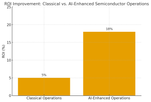
Figure 2. Firms adopting AI-enhanced semiconductor operations achieve significantly higher ROI, with consulting studies reporting double-digit efficiency gains compared to classical operations.
At the end of the day, companies that successfully integrate these technologies do not just
bring products to market faster; they also gain a genuine competitive edge in today’s unpredictable global markets. In the semiconductor industry, a delay of a few weeks can result in billions in lost revenue, so agility is essential for survival.
Future Outlook: Scaling Quantum AI Impact on Semiconductor Manufacturing
Looking ahead, the next major development appears to be full-stack quantum-AI design.
Imagine quantum processors running full-chip simulations while AI optimizes them for
speed, efficiency, and manufacturability. Although we are not there yet, incremental
advances in photonic circuits and spintronic components are already producing tangible
results.
For manufacturing teams, the challenge will be maintaining flexibility in supply chains. As
new materials move from simulation to pilot production, procurement and fab teams must
scale in coordination. Today’s quantum processors are not perfect, as they still face
limitations in qubit counts, error rates, and scalability, but if progress continues, practical
industrial applications could emerge within the next ten years. Companies that begin planning now, by developing roadmaps and forming strategic partnerships, will gain a significant advantage.
Conclusion
Right now, the semiconductor industry is at a critical turning point. Combining AI’s
predictive capabilities with quantum computing’s atomic-level insights can accelerate
discovery, shorten lead times, and make supply chains significantly more resilient.
For engineers and procurement leaders, the message is clear: adopting AI-quantum
integration is not just about technology; it is about remaining competitive. The next major
advancement in silicon will not occur by chance. It will be carefully designed, optimized, and engineered using AI and quantum computing together.
The post The Quantum Leap: How AI and Quantum Computing Are Driving Lead Time Optimization and Supply Chain Resilience in Semiconductor Innovation appeared first on ELE Times.
Rohde & Schwarz Mobile Test Summit 2025 on the future of wireless communications
Rohde & Schwarz has announced that this year’s Mobile Test Summit will be an online, multi-session event catering to two major time zones. Wireless communications professionals are invited to register for individual sessions on the Rohde & Schwarz website. The sessions will cover a wide range of critical industry topics: AI and machine learning in mobile networks, non-terrestrial networks (NTN) for mobile devices, the transition from 5G to 6G and the next generation of Wi-Fi.
- The first topic, AI and machine learning, will cover how AI and ML are changing mobile networks.
- The second topic is NTN, and its sessions will cover how the evolving NTN landscape enhances the mobile user experience and provides true global coverage for IoT devices.
- The third topic addresses the transition from 5G to 6G, with a focus being on XR applications in the 6G age, new device types and the rise of private 5G NR networks. Special focus will be on the impact on test and measurement as the industry evolves from 5G to 6G.
- The fourth topic covers the latest advancements in Wi-Fi 8 technology and how they elevate the mobile user experience.
Alexander Pabst, Vice President of Wireless Communications at Rohde & Schwarz, says: “As we mark the fifth anniversary of hosting our popular Mobile Test Summit, we’re excited to continue this open forum for the global wireless community to exchange ideas, share experiences and debate the technical and operational questions that will shape the future of connectivity. The virtual, multi‑session format makes it easy for professionals in the wireless ecosystem around the globe to participate in focused conversations and obtain actionable insights that help shape the industry’s future.”
The post Rohde & Schwarz Mobile Test Summit 2025 on the future of wireless communications appeared first on ELE Times.
Pages

