
ELE Times

Rethinking AI Networking: Myths vs. Reality
As artificial intelligence infrastructure scales at breakneck speed, outdated assumptions about networking continue to circulate. Many of these myths stem from technologies designed for much smaller clusters, but the game has changed. Today’s AI systems are pushing into hundreds of thousands and soon, millions of GPUs. Old models simply don’t hold up.
Let’s take a closer look at the most persistent misconceptions about AI networking and why Ethernet has clearly established itself as the foundation for modern large-scale training and inference.
Myth #1: Ethernet Can’t Deliver High-Performance AI Networking
This one’s already been disproven. Ethernet is now the standard for AI at scale. Nearly all of the world’s largest GPU clusters built in the past year use Ethernet for scale-out networking.
Why? Because Ethernet now rivals and often outperforms alternatives like InfiniBand, while offering a stronger ecosystem, vendor diversity, and faster innovation. InfiniBand wasn’t designed for the extreme scale we see today; Ethernet is thriving with 51.2T switches in production and Broadcom’s new 102.4T Tomahawk 6 setting the pace. Massive clusters of 100K GPUs and beyond are already running on Ethernet.
Myth #2: You Need Separate Networks for Scale-Up and Scale-Out
That was true when GPU nodes were tiny. Legacy scale-up designs worked when you were connecting two or four GPUs. But today’s architectures often include 64, 128, or more GPUs within a single domain.
Using separate networks adds complexity and cost. Ethernet allows you to unify scale-up and scale-out on the same fabric, simplifying operations and enabling interface fungibility. To accelerate this convergence, we introduced the Scale-Up Ethernet (SUE) framework to the Open Compute Project, moving the industry toward a single AI networking standard.
Myth #3: Proprietary Interconnects and Exotic Optics Are Essential
Not anymore. Proprietary approaches may have fit older, fixed systems, but modern AI requires flexibility and openness.
Ethernet provides a broad set of choices: third-gen co-packaged optics (CPO), module-based retimed optics, linear drive optics, and long-reach passive copper. This flexibility lets you optimize for performance, power, and economics without being locked into a single path.
Myth #4: Proprietary NIC Features Are Required for AI Workloads
Some AI clusters lean on programmable, high-power NICs for features like congestion control. But often, that’s compensating for a weaker switching fabric.
Modern Ethernet switches, including Tomahawk 5 and 6, already embed advanced load balancing, telemetry, and resiliency — reducing cost and power draw while leaving more resources available for GPUs and XPUs. Looking ahead, NIC functions will increasingly integrate into XPUs themselves, reinforcing the strategy of simplifying rather than over-engineering.
Myth #5: Your Network Must Match Your GPU Vendor
There’s no reason to tie your network to your GPU supplier. The largest hyperscaler deployments worldwide are built on Ethernet.
Ethernet enables flatter, more efficient topologies, supports workload-specific tuning, and is fully vendor-neutral. With its standards-based ecosystem, AI clusters can scale independently of GPU/XPU choice-ensuring openness, efficiency, and long-term scalability.
The Takeaway:
Networking is no longer a side note; it’s a core driver of AI performance, efficiency, and growth. If your assumptions are rooted in five-year-old architectures, it’s time to update your playbook.
The reality is clear: the future of AI networking is Ethernet and that future is already here.
(This article has been adapted and modified from content on Broadcom.)
The post Rethinking AI Networking: Myths vs. Reality appeared first on ELE Times.
Why Electronics and Auto Manufacturers Struggle with Compliance in India
Electronics and automobile manufacturers, contributing 3% and 7.1% to India’s GDP respectively, are at the heart of the nation’s industrial growth. Yet, their progress is often slowed by a maze of compliance requirements from evolving labour codes and plant safety regulations to environmental certifications and state-specific laws. For many players, these overlapping obligations translate into delays, operational inefficiencies, and missed opportunities to scale.
To understand how compliance challenges are shaping the future of these sectors, and how technology like AI and RPA is redefining compliance management, ELE Times spoke with Munab Ali Beik, Head of Compliance Advisory at Core Integra. With over 20 years of experience navigating regulatory frameworks and driving digital compliance transformations, he provides deep insights into the hurdles manufacturers face, the reforms needed to unlock growth, and how smart compliance practices can strengthen India’s position as a global manufacturing hub.
Excerpts from the interview:
ELE Times: What are the most complex compliance requirements currently troubling electronics and automobile manufacturers in India?
Munab Ali Beik: For electronics and automobile manufacturers, the most complex compliance challenges today revolve around evolving labour laws, contractor & supplier compliances, shop floor regulations, health and safety requirements, unions and employee welfare norms. With the introduction of upcoming new labour codes, companies must realign HR policies, wage structures, obtaining registrations and working hours while maintaining strict adherence to health and safety standards. Shop floor compliance has become increasingly demanding, requiring detailed SOPs, audits, and documentation to manage risks associated with heavy machinery. Beyond this, manufacturers face intricate requirements around plant certifications, environmental regulations, product safety standards, certifications, audits and overall labour law compliance. Studies indicate that nearly 45–50% of players’ experience delays and operational inefficiencies due to these overlapping regulatory demands, highlighting the critical need for proactive compliance management.
ELE Times: Why do almost half of manufacturers experience delays specifically due to compliance hurdles?
Munab Ali Beik: The delay is due to compliance hurdles because the regulatory landscape remains highly complex and fragmented. Frequent updates to labour laws and enterprise laws require constant adjustments, while machinery safety norms and employee welfare provisions add operational challenges. For companies operating multiple plants, the lack of uniformity across states further complicates compliance, state-specific laws, local regulatory requirements, and varying environmental norms necessitate separate processes and documentation. States have indicated that the Ease of Doing Business initiative may complicate the procedural implementations and understanding the simplified part of compliances. This patchwork of regulations, combined with limited coordination across jurisdictions, creates bottlenecks and inefficiencies, slowing operations and impacting manufacturers’ ability to scale effectively.
ELE Times: With electronics contributing 3% and automobiles 7.1% to India’s GDP, do you think regulatory overload is limiting their full growth potential?
Munab Ali Beik: Yes, absolutely. If compliance hurdles were streamlined, electronics and automobile manufacturers could devote far more resources to R&D, innovation, and building global competitiveness. These sectors have the potential to not only sustain but significantly increase their contribution to India’s GDP by boosting exports, enhancing localization, and developing advanced manufacturing ecosystems. Procedural bottlenecks currently divert focus from scaling production, investing in cutting-edge technologies, and optimizing supply chains. While India is making strides in improving ease of doing business, attracting larger foreign investments and sustaining growth requires simpler and more stable compliance frameworks. The central and state governments are set to relax certain provisions for the electronics and automobile manufacturing sectors to improve their performance. These relaxations pertain to auto-renewals, inspections, self-certifications, working hours, overtime, industrial disputes, subsidies, and promotional activities. Reducing regulatory overload would enable these industries to strengthen core operations, accelerate India’s emergence as a global manufacturing hub, and unlock untapped economic potential.
ELE Times: How can AI and RPA truly transform compliance management for manufacturing plants?
Munab Ali Beik: AI and RPA can revolutionize compliance management in manufacturing by automating repetitive tasks like payroll, attendance tracking, statutory filings, registers maintenance, returns filing, maintaining the data, Management information system and audit reporting. AI platforms provide real-time visibility, flag risks, and update changes in regulations automatically, while RPA ensures consistent workflows across HR, finance, and operations. This reduces errors, boosts efficiency, and frees management to focus on strategic priorities. Over time, digital compliance not only cuts costs, increase the efficiency, error free and improves safety monitoring but also strengthens governance and investor confidence.
ELE Times: What critical changes are required to make India a global manufacturing hub for electronics and automobiles?
Munab Ali Beik: To position India as a global manufacturing hub for electronics and automobiles, critical changes are needed in regulatory stability, ease of doing business, exemption from regulatory frameworks and policy clarity. Simplifying access to government schemes, enhancing transparency in labour laws, and streamlining compliance processes will reduce operational friction and build investor confidence. These measures will enable manufacturers to focus on innovation, scale efficiently, and compete globally, driving both domestic growth and export potential.
ELE Times: How is Core Integra evolving its AI/RPA tools to stay aligned with future compliance expectations?
Munab Ali Beik: We are continuously enhancing our AI and RPA capabilities through our compliance platform, Ctrl F, to stay ahead of evolving regulatory requirements. We leverage AI to track changing laws in real time, identify the impacts, flag risks, and automate documentation, filings, and reporting. By integrating RPA, we ensure consistency across multi-location operations, reduce manual errors, simplified the process and minimize administrative burdens. Alongside technology, we invest in R&D and advisory expertise to simplify complex regulations and provide proactive compliance updates. These innovations empower our clients to manage compliance efficiently, enhance operational oversight, and focus resources on scaling and innovation.
The post Why Electronics and Auto Manufacturers Struggle with Compliance in India appeared first on ELE Times.
Unlocking the Power of AI: A Strategic Guide for OEMs and ISVs
Artificial intelligence is no longer some faraway notion; it has become a strong and immediate agent of innovation. Whether in predictive analytics or generative design, AI remains instrumental in the means by which OEMs and ISVs conceive, produce, and maintain their products. However, promising this technology is, majority of companies cannot speed away from experimentation into value-driven and large-scale application.
This guide demystifies the AI technologies reshaping the industry, illuminates their real-world applications, and lays down a commercially viable roadmap for OEMs and ISVs to embrace AI with confidence and clarity.
Understanding Artificial Intelligence
AI refers to the development of computer systems capable of performing tasks traditionally requiring human intelligence. These systems process vast amounts of data, recognize patterns, and make decisions with minimal human intervention. AI spans a wide spectrum from rule-based automation to advanced deep learning algorithms capable of generating content, interpreting speech, and predicting outcomes.
While AI has existed for decades, the surge in computational power, cloud infrastructure, and data availability has accelerated adoption across industries. Today, AI is no longer optional it is an essential enabler for companies striving to remain innovative and competitive.
The Different Types of AI:
Natural Language Processing (NLP)
NLP enables machines to understand, interpret, and generate human language. It powers chatbots, virtual assistants, translation tools, and sentiment analysis systems. OEMs and ISVs are integrating NLP into products to create voice-enabled interfaces, enhance customer engagement, and extract insights from unstructured data such as emails, reviews, and social media.
Machine Learning and Predictive Analytics
Machine Learning (ML) allows systems to learn patterns from data and make predictions without explicit programming. Predictive analytics, a major ML application, helps anticipate trends, detect anomalies, and optimize operations. For instance, predictive maintenance reduces downtime by forecasting equipment failures, while cybersecurity solutions use ML to detect threats in real-time.
Generative AI
Generative AI is the next frontier. Unlike traditional ML, it creates new content—ranging from text and images to design prototypes. For OEMs and ISVs, this translates into automated documentation, rapid product prototyping, and personalized customer experiences. Generative AI not only streamlines workflows but also fosters creativity and innovation.
Addressing the Challenges of AI Adoption:
Despite its potential, AI adoption comes with hurdles-
Bias and Fairness: AI models trained on biased datasets risk producing unfair or inaccurate outcomes. Businesses must prioritize transparency and accountability in AI systems.
Integration Complexity: Legacy infrastructure, siloed data, and fragmented workflows often complicate AI integration.
Data Security and Privacy: AI systems process sensitive business and customer information, making strong data governance and compliance with privacy regulations critical.
Continuous Adaptation: AI models require constant monitoring, retraining, and refinement to remain accurate in dynamic business environments.
Deploying AI Strategically for OEMs and ISVs:
To move beyond pilots and achieve scalable impact, businesses should approach AI strategically:
- Align AI with Business Goals – Identify specific areas where AI can enhance value, such as automation, customer engagement, or operational efficiency.
- Ensure Data Readiness – High-quality, structured data is the backbone of AI success. Companies must invest in robust data collection and management systems.
- Leverage Cloud and AI-as-a-Service – Cloud-based platforms lower barriers to entry by offering scalable AI tools without requiring deep in-house expertise.
- Collaborate with AI Experts – Partnering with specialized providers accelerates adoption and optimizes solutions for industry-specific needs.
- Commit to Continuous Improvement – Regularly monitor performance, retrain models, and evolve AI capabilities alongside business needs.
The Future of AI in Business:
AI’s evolution is accelerating. Explainable AI (XAI) is enhancing transparency, allowing businesses to understand and trust AI-driven decisions. Edge AI is bringing intelligence closer to data sources, enabling real-time decision-making in IoT and remote deployments. Together, these innovations are making AI more practical, ethical, and impactful.
For OEMs and ISVs, investing in AI today is not just about keeping pace it’s about leading the transformation. Those who strategically integrate AI will unlock new opportunities in product development, customer engagement, and operational efficiency, securing a decisive competitive edge.
Conclusion:
AI is no longer experimental it is a strategic imperative. From NLP-driven customer engagement to predictive maintenance and generative design, the opportunities for OEMs and ISVs are vast. By aligning AI adoption with business goals, addressing data and integration challenges, and committing to continuous refinement, companies can unlock the full potential of AI.
(This article has been adapted and modified from content on Arrow Electronics.)
The post Unlocking the Power of AI: A Strategic Guide for OEMs and ISVs appeared first on ELE Times.
Electronica India and productronica India 2025: India’s Powerplay in Electronics, set to propel the future of electronics manufacturing
- Marking the event’s biggest international participation to date, the edition brings together 6,000+ global brands from over 50 countries, featuring pavilions from Germany, Japan, Taiwan, and more.
- A dynamic meeting ground for collaboration and innovation spanning Start-Up and SME zones, conferences, podcasts, forums, and buyer–seller programs.
- Cricket icon Rohit Sharma leads the campaign, embodying India’s spirit of innovation, teamwork, and emerging global leadership in electronics.
India is steadily strengthening its position in the global electronics landscape, moving from being a participant to becoming a key driver of innovation and manufacturing. This momentum comes to life at the co-located trade fairs, electronica India and productronica India, returning to the Bangalore International Exhibition Centre (BIEC) from 17–19 September 2025.
This year’s edition reflects the scale of India’s electronics growth journey. Spread across 60,000 square meters, the fairs will feature 6,000+ global brands and participation from 50+ countries. From semiconductor design and embedded systems to electronic components and production technologies, the platform will spotlight innovations driving electric mobility, smart displays, and Industry 4.0, reinforcing India’s growing role in global electronics manufacturing.
In a move that links national pride with technological prowess, cricket icon Rohit Sharma has been named the face of the event, embodying the theme, “India’s Powerplay in Electronics.” It’s a fitting analogy Sharma’s leadership, innovation, and teamwork on the field resonate with the very ethos driving India’s electronics sector.
Bhupinder Singh, President IMEA, Messe München and CEO, Messe Muenchen India, said:
“These trade fairs underscore India’s global ambitions in electronics manufacturing. This year marks a record international participation for the event, with representation from over 50 countries and dedicated pavilions from Germany, Japan, Taiwan, and more. The platform brings together industry leaders, policymakers, and innovators to advance design-led innovation and modern manufacturing. With Rohit Sharma as the face of this edition, they embody the scale, energy, and vision driving India’s Powerplay in Electronics.”
Dr. Reinhard Pfeiffer, CEO of Messe München, added:
“The significance of these trade fairs lies in uniting every layer of the electronics ecosystem from global industry leaders to agile startups, from government stakeholders to academia. Hosting this convergence in Bengaluru underscores India’s fast rise as a key technology hub and its growing influence on global innovation trends. For Messe München, this edition represents a milestone in our mission to foster cross-border collaboration and create a truly global platform for innovation and growth.”
The event’s gravitas is underscored by powerful alliances with Government of Karnataka as State Partner and support from premier industry associations including the Electronic Industries Association of India (ELCINA), India Cellular & Electronics Association (ICEA), Electronics City Association ofIndia (ELCIA), Consortium of Electronic Industries in Karnataka (CLIK), Taiwan Printed Circuits Association (TPCA), Korea Printed Circuits Association (KPCA) and Global Industry Association (GEA) other association names.
Rajoo Goel, Secretary General of ELCINA, underscores:
“What excites us is the balance between today’s opportunities and tomorrow’s vision. With pioneering start-ups, global pavilions, semiconductor design focus, extensive representation of components and materials value chain as well as buyers and sellers converging, these trade fairs reflect the fast maturity of our industry. ELCINA is proud to partner in building an ecosystem where policy, innovation, and collaboration come together and where India’s electronics manufacturing is stepping into genuine global leadership.”
At the heart of this year’s buzz are 18 pioneering start-ups, backed by the Government of Karnataka and Startup Karnataka, unveiling breakthrough innovations across the electronics value chain and highlighting India’s deep-tech and semiconductor strength. Adding momentum, the India Semiconductor Conclave will convene global leaders and policymakers to drive India’s design-led chipmaking ambitions onto the world stage.
Karnataka Innovation and Technology Society expressed pride in supporting electronica India and productronica India 2025 in Bengaluru. This support underscores Karnataka’s commitment to advancing a design-led and manufacturing-led future in electronics and semiconductors. By fostering innovation, attracting global investments, and empowering start-ups, the state continues to create an environment where technology thrives, talent flourishes, and India strengthens its position as a global leader in electronics. electronica India and productronica India 2025 will go beyond traditional displays with:
- Innovation Forum – spotlighting breakthrough ideas in sustainability, Japanese tech trends, asset tracking, e-tolling, and future navigation.
- Buyer–Seller Forum – driving 2,000+ structured meetings with procurement leaders from Honda, Pricol, BHEL, BEL, Lava, Foxconn, and more across PSUs, automotive, consumer electronics, mobility, and industrial sectors.
- Industry-led Conferences – a series of focused forums including the CEO Forum, eFuture, eMobility, Capital Goods & Automation, India PCB Tech, and the India Semiconductor Conclave.
- Live Podcast Series – featuring conversations with industry thought leaders and innovators, adding dialogue to the show floor.
Together, these programmes blend demonstration, deal-making, and dialogue—underscoring India’s Powerplay in Electronics as it ignites Bengaluru.
The post Electronica India and productronica India 2025: India’s Powerplay in Electronics, set to propel the future of electronics manufacturing appeared first on ELE Times.
Power Electronics Market Trends: SiC & GaN Technologies Reshape Industry Outlook
The power electronics sector is set to start a final stage of growth as it is expected to have an evaluated market value of USD 51.73 billion by 2025, reaching USD 67.42 billion by 2030. A steady CAGR of 5.4% stems from a steady increase in demand for energy efficiency, renewable integration, and semiconductor advanced technology.
The Growth Drivers:
The positive momentum of the market is born out of interlinked phenomena:
Clean Energy Imperative
As the world tries to go carbon-neutral, renewable energy systems, including solar photovoltaic and wind farms, go mainstream. Power electronics, hence, are used in these systems to enable efficient energy conversion, grid integration, and real-time management.
Electrification of Transport
With EVs and HEVs no longer considered niche, the demand is now rising for high-performance inverters, converters, and battery-management systems. The transition is fueled by policy, consumer interest, and vehicle-electrification technology advances.
Semiconductor Innovations
Wide-bandgap materials such as silicon carbide (SiC) and gallium nitride (GaN) are reshaping design possibilities. These materials enable devices that are smaller, faster, more efficient, and capable of operating at higher temperatures making them invaluable for modern automotive, industrial, and renewable applications.
Smart Infrastructure and Connectivity
With the development of smart grids, connected mobility, and smart manufacturing, there is a greater demand for the precision operation of power. Power electronics underpin these systems to foster efficiency, safety, and interoperability.
Though on a positive trending path, the sector faces engineering challenges, chiefly in the design and packaging of SiC devices, which mandate careful thermal and structural management.
Market Segmentation Insights:
Automotive & Transportation: Fastest Growing Segment
This industry segment shall witness the highest CAGR during the forecast period. Vehicle electrification, growing ADAS features, integration of infotainment systems require advanced power electronics focusing on efficiency and reliability, which are only further underlined with the march toward autonomous and connected vehicles.
Power ICs: Market Leader
Power ICs will maintain their position as the largest share commanded due to their extensive uses in consumer electronics like smartphones, laptops, and tablets; industrial and automotive applications. They become vital for reducing energy loss, extending battery life, ensuring high performance, and reliability of systems.
Regional Insights:
Asia-Pacific region is considered to be the center of the global market and hence is projected to remain dominant. The key drivers behind its domination are:
Percentagewise: Strong power electronics manufacturing systems in China, Japan, South Korea, and Taiwan.
Rapid urbanization and industrialization in emerging economies such as India, Vietnam, and Indonesia.
Generous government aids for the adoption of EVs and the deployment of renewable energy.
Asia Pacific then stands as a global supplier and a major consumer of power electronics, given the establishment of an industrial base and growing domestic demand.
Industry Panorama:
The market consists of well-established technology giants as well as specialized players. Major companies include Infineon Technologies AG, Texas Instruments Incorporated, ON Semiconductor, STMicroelectronics, Analog Devices, Inc., Mitsubishi Electric Corporation, Renesas Electronics Corporation, Toshiba Corporation, Fuji Electric Co., Ltd., and Vishay Intertechnology, Inc.
Such firms intend to strengthen their market positions with product innovations, partnerships, acquisitions, and increased capacity. Investing heavily in R&D with special emphasis on SiC and GaN technologies, they are shaping the next generation of energy efficient systems.
Future Outlook:
Power electronics’ contribution to a cleaner, smarter, and more connected society will define the market by 2030. The industry is situated at the nexus of technological innovation and energy change, powering everything from electric vehicles to regulating renewable energy flows and supporting the gadgets we use on a daily basis.
In this situation, businesses that can expand production, overcome material constraints, and innovate for efficiency will not only prosper but also establish the standards for a sustainable electronics future.
The post Power Electronics Market Trends: SiC & GaN Technologies Reshape Industry Outlook appeared first on ELE Times.
Analog Electronics: The Timeless Backbone of Modern Sensors
Introduction: The “Old” Tech Powering the “New” World
In today’s electronics ecosystem, conversations are dominated by artificial intelligence, edge computing, and ultra-fast wireless networks. Yet, behind every groundbreaking innovation, there lies a quieter but indispensable player i.e., analog electronics. While digital may dominate headlines, it is analog that ensures real-world phenomena which can be captured, conditioned, and processed.
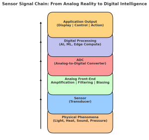
As engineers often remind themselves, “Nature is analog. Everything else is an approximation.” No matter how sophisticated a digital system is, its accuracy and reliability hinge on the quality of the analog front-end. From radar in advanced driver-assistance systems (ADAS) to MEMS accelerometers in smartphones, and from biomedical wearables to industrial IoT nodes, analog electronics forms the first link in the sensor signal chain.
Why All Sensors Speak Analog First
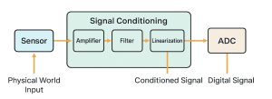
Every physical phenomenon light intensity, sound waves, heat, vibration, or radio frequency (RF) radiation exists in analog form. Sensors are essentially transducers, converting these continuous signals into measurable electrical quantities. But before such data can be digitized and analyzed by processors or AI algorithms, it must pass through an analog front-end (AFE).
The AFE includes key blocks such as instrumentation amplifiers, filters, linearization circuits, and signal conditioning modules that prepare raw sensor outputs for analog-to-digital conversion (ADC). Without robust analog conditioning, even the most advanced digital processors would be “blind” to the real world.
As Walt Maclay, CEO of Voler Systems, puts it: “Digital processing is only as good as the analog electronics feeding it. Garbage in, garbage out applies more to sensors than anywhere else.”
Core Functions of Analog in Modern Sensors
- Signal Amplification
Many sensors output signals in the microvolt or millivolt range, easily drowned by noise. Instrumentation amplifiers and low-noise amplifiers (LNAs) boost these signals while preserving fidelity. For example, electrocardiogram (ECG) sensors require amplifiers with high common-mode rejection ratios (CMRR) to extract meaningful heart signals from noise-laden environments. - Filtering
Real-world signals are messy. Analog active and passive filters remove unwanted noise and interference before digitization. In radar systems, bandpass filters ensure only the target frequency range is processed, dramatically improving signal-to-noise ratio (SNR). - Linearization & Biasing
Many sensor outputs are nonlinear by nature. Analog circuits implement linearization techniques that correct these distortions, making sensor behavior predictable. Similarly, biasing ensures transducers operate in optimal ranges. For example, in thermistors, resistance-to-temperature curves must be linearized before meaningful temperature data is derived. - Conversion Readiness
Analog circuits prepare signals for ADC compatibility by ensuring proper voltage levels, impedance matching, and bandwidth. Without this step, digitization could lead to clipping, aliasing, or resolution loss.
Case Studies: Analog at Work in Emerging Applications
- Automotive ADAS
ADAS relies heavily on radar and LiDAR sensors, where real-time performance is non-negotiable. Analog front-ends amplify weak RF echoes, filter them for interference, and feed precise signals to high-speed ADCs. Even a microsecond delay can mean the difference between safe braking and a collision.
- Biomedical Devices
Wearable medical devices like glucose monitors and ECG patches demand ultra-low-power, high-precision analog circuits. Here, analog electronics extend battery life while ensuring clinical-grade accuracy. An error of even 1 mV in amplification could translate into misdiagnosis.
- Industrial IoT
Factories rely on thousands of sensors for vibration monitoring, predictive maintenance, and process automation. Analog circuits in these environments must withstand electrical noise, temperature fluctuations, and mechanical stress. Unlike fragile digital logic, robust analog designs ensure reliability under extreme industrial conditions.
- Environmental Monitoring
Long-term stability is critical in air-quality monitors, soil sensors, or weather stations. Analog circuits designed for low drift and high linearity guarantee consistent data for years without recalibration.
Analog’s Edge Over Digital in Certain Tasks
While digital processing offers flexibility, analog holds an edge in critical aspects:
- Zero Latency: Analog signals propagate at the speed of physics — no clock cycles required. For radar-based collision avoidance, this deterministic performance is irreplaceable.
- Power Efficiency: Analog front-ends consume far less power than equivalent digital circuits, making them essential in wearables and IoT nodes where every microamp counts.
- Reliability under Harsh Conditions: Analog circuits continue functioning in extreme environments — radiation, high temperatures, or electromagnetic interference — where digital logic often fails.
As Bob Dobkin, co-founder of Linear Technology, famously said: “Analog will never die, because the world is analog.”
Integration Trends: Analog in the Age of SoCs and SiPs
The industry is increasingly moving towards system-on-chips (SoCs) and system-in-packages (SiPs) that integrate both analog and digital functions. For instance, today’s MEMS inertial sensors often include on-chip AFEs, ADCs, and digital processors in a single package. This integration reduces footprint, improves signal integrity, and supports miniaturization for wearables, drones, and autonomous systems.
However, integration does not eliminate the need for analog expertise. Instead, it requires engineers to design mixed-signal systems where the interplay between analog and digital domains is carefully managed. Issues like thermal drift, bandwidth matching, and parasitic effects remain squarely in the analog domain.
Conclusion: Analog as the Permanent Foundation
In the race towards digital transformation, analog electronics is often overlooked. Yet, it is precisely analog that determines how effectively digital systems can sense and respond to the physical world. Whether in self-driving cars, medical diagnostics, or industrial automation, analog remains the timeless backbone of modern sensors.
For engineers, the message is clear: mastering analog design is not a relic skill, but a future-proof investment. The more complex and interconnected systems become, the more critical it is to ensure rock-solid analog foundations.
As the electronics pioneer Barrie Gilbert once noted: “You can digitize data, but you cannot digitize reality. Reality is, and will always be, analog.”
The post Analog Electronics: The Timeless Backbone of Modern Sensors appeared first on ELE Times.
Generative Artificial Intelligence Boosts Chip Yields and Slashes Manufacturing Defects
In 2021, car manufacturers worldwide halted production because a single one-dollar microcontroller was unavailable. The wait time for advanced semiconductors jumped from 12 weeks to over 26 weeks, revealing how fragile the global supply chain had become. The yield losses and manufacturing defects are not just technical issues-they are strategic challenges affecting procurement leaders, supply chain managers, and even national economies.
Meanwhile, demand for semiconductors continues to grow relentlessly. Global consumption is expected to increase at a compound annual growth rate of 7 to 8 percent through 2030, while production capacity is only growing at about 5 percent per year. This mismatch makes every wafer incredibly valuable. Even a modest 2 percent improvement in yields at advanced technology nodes could free up around 150,000 wafers annually, which translates into billions of dollars of extra supply.
Generative AI addresses these challenges by creating optimized designs in advance, anticipating potential defects, and enhancing scheduling in wafer fabrication. It is reshaping the economics of the semiconductor industry- improving yields, reducing inconsistencies, and strengthening supply chains’ reliability.
The Yield Challenge in Semiconductor Manufacturing
Chip manufacturing involves more than 1,000 steps, from photolithography to etching. At advanced nodes of three nanometres and below, tiny atomic-level variations can make wafers unusable. With single-wafer costing over 16,000 dollars, any loss in yield directly cuts profit margins.
Every percentage point of yield improvement is like adding a new fabrication plant without capital investment, said Sanjay Mehrotra, CEO of Micron Technology.
How Generative AI Creates Strategic Value
Generative models such as Generative Adversarial Networks (GANs), Variational Autoencoders (VAEs), and foundation models go beyond predictive analytics: they generate better alternatives. Four applications stand out:
- Design Optimization
Generative AI evaluates thousands of layout variations to identify configurations that reduce defects. Synopsys, working with Taiwan Semiconductor Manufacturing Company (TSMC), reported a 15 percent yield improvement using AI-driven design space exploration. Faster design cycles and quicker delivery to customers follow. A European fabless design company leveraged generative AI for design optimisation and achieved ROI in just 18 months, reducing wafer scrap, accelerating revenue realization, and lowering operational costs.
- Defect Prediction
AI generates synthetic wafer maps to train inspection systems before defects appear. American-based KLA corporation reported 25–30 percent improvement in defect detection, resulting in more usable wafers and faster production cycles. Samsung implemented AI-based yield learning to cut line failure rates by 12 percent, decreasing buffer inventory needs and improving delivery reliability.
- Assistance with Lithography
AI supports mask patterns generation to minimize distortions through Inverse Lithography Technology (ILT) and Optical Proximity Correction (OPC). Intel reported a 40 percent reduction in edge-placement error, increasing first-pass yields.
- Supply Assurance and Fabric Scheduling
Generative AI simulates thousands of scheduling scenarios, balancing tool usage, and maximizes throughput. A Taiwanese fabless company reduced wafer cycle times from 20 to 17 days using AI scheduling, ensuring timely chip delivery in a competitive market.
It also strengthened broader supply chain resilience. Global Foundries applied predictive analytics to reduce recovery times during material shortages by 30 percent, helping procurement meet client demand during disruptions.
Industry Case Studies and Outcomes
- Samsung Foundry – AI-based Yield Learning- It reduced the cut line failure rates by 12 percent, lowering buffer inventory requirements and improving delivery reliability for customers.
- Global Foundries – Predictive Supply Chain Analytics: Using predictive analytics, it improves supply chain resilience and cuts recovery times during material shortages by 3 percent, enabling procurement teams to meet client demands.
- European Fabless Design Company – Design Optimisation: Employing generative AI for layout optimisation, the company achieved return on investment (ROI) in just 18 months. By decreasing wafer scrap, speeding revenue realisation, and reducing operational cost.
Strategic Procurement and Supply Chain Value
Generative AI serves the dual role. On the shop floor, it functions like examining billions of flaw patterns to increase yields. In the boardroom, it mitigates risk, strengthens supply continuity, and protects margin.
Predictive insight facilities by generative AI can help with lead time optimisation, multi-sourcing strategy guidance, and supplier negotiations, and align contractual requirements with actual fab performance, ensuring reliable capacity guarantees.
SEMI CEO Ajit Manocha stated that generative AI is not just yield enhancement-, it lowers process variability, increases predictability, and strengthens overall operational resilience.
Challenges to Adoption
Despite its transformative potential, adopting generative AI in the semiconductor industry presents several challenges:
Ø Data confidentiality: It remains the key concern because the processed data is so proprietary and difficult to share across ecosystems.
Ø Computational intensity: It requires a substantial amount of computational equipment to train sophisticated AI generative models.
Ø Explainability gaps: To foster confidence, engineers and procurement teams need AI advice to be transparent.
Ø Change management: To fully realise value, Fabs must retrain process engineers, educate procurement specialists in AI literacy, and link data science teams across silos.
The Road Ahead: Toward Autonomous and Resilient Fabs
Next-generation semiconductor factories are increasingly relying on generative AI as central intelligence. Emerging trends include:
- Autonomous fabs: It leverages generative AI to modify recipes in real time to reduce yield loss and improve efficiency.
- Collaborative ecosystems: Design firms, equipment manufacturers, and fabs share AI models to optimize production and supply chain resilience.
- Zero-defect manufacturing: While idealistic, generative AI is making substantial progress towards achieving it, bringing fabs closer to near-perfect yield and consistency.
Strategic Imperatives for Leaders
The path forward is clear for procurement executives, semiconductor leaders, and strategy decision makers:
- Scale AI across operations: Transition from pilots to full integration in scheduling, lithography, electronic design automation, and inspection workflow.
- Leverage AI in procurement: Use insights for contract negotiations, supplier diversification, and lead time predictability.
- Invest in people and collaborations: Integrate the expertise of supply chain managers, data scientists, and strengthen collaboration with AI solution providers and academic institutions.
Conclusion
Generative AI is transforming chip manufacturing. It boosts yields, cuts defects, and improves production scheduling. More importantly, it helps leaders make supply chains stronger, margins steadier, and delivery times more predictable.
Companies that embrace AI first will unlock extra capacity, protect supply continuity, and gain a clear competitive edge. Every wafer counts, and every week of lead time matters. Generative AI ensures neither is wasted.
The post Generative Artificial Intelligence Boosts Chip Yields and Slashes Manufacturing Defects appeared first on ELE Times.
Welcome to the Indian era of global technology
India is emerging as the big Global South trade story as it pursues favorable relations with most of the world’s major economies. Simultaneously, it has highlighted the complexity and fragility of the global order as the world grapples with intensifying great power competition, the rise of regional actors, and a growing erosion of trust in multilateral institutions. India’s economic growth has been the envy of other nations.
Under this background, Donald Trump issued a strong directive to Silicon Valley’s titans to stop hiring Indians. Why? Because the Indian intellect has evolved from being America’s secret weapon to becoming its most feared competitor. Donald Trump delivering can only be described as a declaration of intellectual war.
Indians – the talent pool and intellectual force has quietly, methodically, and brilliantly infiltrated every corner of American technological supremacy. But without Indian minds, Silicon Valley doesn’t just slow down, it stops. But why are Indians being targeted that have consistently outperformed, out-innovated, and out led every other group in tech space?
The point is that Indians don’t just work in American tech, they run it. Indians constitute just 1% of the U.S. population, yet they represent over 36% of all high-skill immigrant entrepreneurs. They hold 72% of all H-1B visas. They founded more than 25% of billion-dollar startups.
Indians occupy CEO positions at companies worth a combined $2.5 trillion. The intellectual domination speaks itself, Sundar Pichai, Satya Nadella, Shantanu Narayan and Parag Agrawal are the real gems. Indian minds aren’t just participating in America’s tech revolution, they’re leading it.
Under their leadership, these companies haven’t just grown, they’ve transcended their American origins to become truly global forces. And that’s the real threat, because when you can no longer control the minds that drive your most valuable companies, you’ve lost more than economic leverage, you’ve lost technological sovereignty. Here Trump talks about intellectual nationalism and protecting American technology supremacy.
Every major technological breakthrough of the past two decades has Indian fingerprints all over it – be it the rise of artificial intelligence, cloud computing, smartphone revolution and coding the software. This is about intellectual capital that has become irreplaceable. The fear isn’t just about Indian success in America; it’s about India’s independence from America.
Today’s Indian professionals aren’t just seeking American opportunities; they’re creating alternatives to American systems. They’re not just joining tech companies, they’re founding them. They’re not just moving to Silicon Valley; they’re building Silicon Valley back home. Bangalore has become Asia’s tech capital. Indian unicorns are solving problems that American companies haven’t even identified yet. From Paytm revolutionizing digital payments to Flipkart challenging Amazon to Ola competing with Uber, Indian innovation is no longer derivative, it’s original, it’s disruptive, it’s independent.
And the same independence terrifies Trump more than any foreign threat ever could. In such a case you’re no longer the only superpower in the room. You’re just another player in a multipolar game.
Today, India operates its own space program that lands on the moon at a fraction of NASA’s cost. It runs its own digital payment system that processes more transactions than Visa and MasterCard combined. It develops its own AI models trained on Indian languages, solving India’s problems. This is technological independence. The truth is uncomfortable but undeniable.
The Indian mind has become so valuable, so essential, so irreplaceable that even suggesting its absence sends shockwaves through the entire American tech ecosystem. It’s not the beginning of Indian exclusion from American tech. It’s the acknowledgement that Indian inclusion has been so successful, so complete, so transformational, that it now threatens the very narrative of American technological exceptionalism.
Google’s search algorithms, refined by Indian mathematicians, Microsoft’s cloud infrastructure, designed by Indian engineers, Apple’s chip designs, optimized by Indian developers, Amazon’s logistics networks, managed by Indian operations experts, Tesla’s autonomous driving systems, powered by Indian AI researchers are such examples of Indian’s contribution to the US’s technology supremacy. The Indian mind has already reshaped American technology so fundamentally that any attempt to reverse it would be like trying to un-invent the Internet. You can’t separate Indian intelligence from American innovation anymore.
The future belongs to minds that can adapt, innovate, and excel, regardless of geography, politics, or prejudice. The future belongs to talent that creates value wherever it goes and builds bridges wherever it lands. The future belongs to the Indian intellect that has proven its worth. Trump’s fear of Indian talent isn’t India’s problem to solve. It’s America’s competitive disadvantage to manage. Welcome to the new reality. Welcome to the Indian era of global technology.
Devendra Kumar
Editor
The post Welcome to the Indian era of global technology appeared first on ELE Times.
Road to Alternate Battery Solutions: Beyond Lithium for a Sustainable Future
As the world moves towards its ambitious climate friendly goal of net-zero emissions by 2050, transport sector, which contributes between 15% to 25% of total global GHG emissions according to varying estimates, will be closely monitored. Transition from ICE vehicles to Electric Vehicles (EVs) on a large scale is imperative in this regard.
The International Energy Agency (IEA), in its recently released report ‘Global EV Outlook 2025’ estimated that globally, EV sales crossed 17 million in 2024, reaching a sales share of more than 20% of total automotives sold. With China leading the way amounting to half of global electric sales, and new markets emerging in Asia and Latin America, electric cars are expected to exceed a share of 40% of total share by 2030 under current policy settings.
Along with growth in EV sales, the demand for batteries have also gone up, accounting for 950GWh in 2024. The battery makes up about 40% of an EV’s total cost, with lithium as the main element in most batteries worldwide. A Lithium-ion battery (LIB) is made up of a graphite anode, with lithium salt as the electrolyte and a cathode consisting of Lithium compounded with Nickel, Cobalt or Manganese. Consequently, conventional lithium-ion batteries are commonly referred to as NMC batteries, denoting their composition of nickel, manganese, and cobalt.
Supply Chain imbalances of LIBs:
While reserves of these minerals are present in a broad geography of Latin America, Australia, Africa and others, the down stream supply chain of processing and battery manufacturing is heavily skewed in favour of China.

EY research shows China’s hold over processing of EV components encompasses 80-90% of global share. At the same time with giants like CATL, China houses over 70-80% of global LIB manufacturing. Over the years these giants have innovated and reduced the use of Nickel and Cobalt in LIBs and produced Lithium iron phosphate (LFP) batteries on a large scale.
NMC batteries, which are still prevalent in the US and Europe provide an energy density advantage over the LFP batteries, which are in turn cheaper and are widely used in China. The energy density of LFP battery packs is about one-fifth lower by mass (Wh/kg) and one-third lower by volume (Wh/L) than that of NMC battery packs. This advantage, however, is partly offset by LFP’s capability to reach 100% state of charge when required without significant degradation, whereas NMC batteries are typically limited to 80% to preserve long-term performance. The NMC batteries are preferred for operating in colder climates and over long ranges. Whereas enhanced performance level of LFP batteries and the given cost advantages have made them popular in the mass markets.
Global Lithium Constraints:
Primarily Lithium, often referred as ‘white gold’ is extracted from two sources across the globe. Firstly, there are minerals like spodumene, petalite, and lepidolite and secondly from Lithium salts like Lithium hydroxide, Li carbonates and Li chlorides which are highly available in lakes across the Andes mountains.
Parts of Argentina, Bolivia and Chile form the Lithium triangle with large proportion of world’s Lithium reserves. However, an nationalization drive over these reserves seems to proliferate in the Latin American countries, akin to what took place vis-à-vis oil sector with the formation of OPEC in the 1960s introducing new complexities on global supply chains.
Then there is also research going on Absorption type aluminium based direct Lithium extraction, which can reduce water drainage, but such methods are at low Technical Readiness levels (TRL)
Finding a way around the ‘White Gold’:
These dynamics have compelled governments and automakers to look at alternatives to Lithium. Some of the alternate EV battery technologies considered are as follows:
| Battery Technology | Anode Active Material (AAM) | Cathode Active Material (CAM) | Electrolyte |
| Sodium Ion Battery (SIB) | Hard as well as soft Carbon easily available from Crop residue or Agri waste | Sodium ions such as layered oxides | Salts such as sodium hexafluorophosphate (NapF6) |
| Zinc manganese Dioxide battery | Zinc metal, 80% of which globally available is from recycled products | Oxygen from air | Aqueous solution of Potassium hydroxide
(KOH) |
| Aluminium-Air battery | Solid Aluminium metal | Oxygen from air | High pH solution of KOH, NaOH or even NaCl. |
| Hydrogen Fuel Cell (HFC) | Hydrogen gas | Oxygen from air | KOH or NaOH |
The metals other than Lithium that are mostly used in metal ion or metal air batteries are widely available but TRLs of 7-9 as required for commercial EVs are yet not achievable with these technologies. However, technologies like Al-air batteries are inducted in other applications like medical devices. Metal air batteries have higher energy density and lower cost than LIBs but have persistent design challenges.
Batteries with solid electrolytes called solid state batteries are looked upon with high optimism even with low TRLs. Electrolytes used in them are mostly oxides, sulphides or polymer electrolytes.
While HFCs are in use commercially, but their production methods remain debatable. Production of hydrogen through electrolysis of water called green hydrogen is still limited compared to blue hydrogen (produced from methane) and grey hydrogen (produced from capturing hydrogen from fossil fuel).
Reducing Dependence through Recycling
A major source of Raw material extraction is Urban mining, which involves extracting valuable materials from E-Waste contributing to a circular economy. According to Global E-waste monitor, we might see E-waste production levels of 82 million tonnes globally by 2030 providing huge recycling potential. Although inefficient recycling mechanisms hinder urban mining potential. A systematic process of collecting, sorting and dismantling E-waste followed by methods like Pyrometallurgy (Smelting), Hydrometallurgy (Chemical separation) and Biometallurgy (Biological separation) must be integrated at ground level.
It is to be remarked that Alternative battery solutions won’t reduce the share of LIBs and LFPs in EVs immediately just as EVs won’t suddenly replace ICEs on roads. A coordinated strategy working on conventional sources while building resilience through alternatives is the need of the hour for a just climate transition.
The post Road to Alternate Battery Solutions: Beyond Lithium for a Sustainable Future appeared first on ELE Times.
Reimagining Human-Machine Interaction: Force Sensing as the New Frontier in HMIs
Introduction- From Mechanical Inputs to Force-Sensitive Interfaces
Human–Machine Interfaces (HMIs) have transformed dramatically in the past few decades. Early systems relied on mechanical switches, levers, and tactile buttons, robust but limited in design flexibility. The capacitive touch revolution brought sleek glass panels, multi-touch gestures, and sealed surfaces to smartphones, automotive dashboards, and industrial equipment.
However, capacitive technology has well-known drawbacks: poor performance in humid environments, false triggers, difficulty working with gloves, and limited ability to distinguish intentional versus accidental touches. Engineers have long sought the next leap in interaction technology.
That leap is force sensing the ability of HMIs to detect not just whether a surface is touched, but how firmly it is pressed. This evolution unlocks richer interaction, robust operation across challenging environments, and freedom from restrictive material choices. As Dr. Mark Weiser, often regarded as the father of ubiquitous computing, once said:
“The most profound technologies are those that disappear. They weave themselves into the fabric of everyday life until they are indistinguishable from it.”
Force sensing is enabling precisely this an interaction layer so intuitive and adaptable that it becomes invisible, yet indispensable.
Technology Fundamentals- How Force Sensing Works
Force sensing is fundamentally about converting mechanical load into an electrical signal. Two primary sensing principles dominate the market: piezoresistive and capacitive force sensing.
Piezoresistive Force Sensors
- Operate by measuring a change in electrical resistance when a material deforms under load.
- Typically use a full-bridge Wheatstone configuration, where four resistive elements form a balanced circuit.
- When force is applied, resistance changes unbalance the bridge, producing a measurable voltage signal.
- Advantages: High sensitivity, strong signal-to-noise ratio (SNR), good temperature compensation, suitability for MEMS fabrication.
- Considerations: Requires calibration to account for long-term drift and environmental conditions.
Capacitive Force Sensors
- Detect changes in capacitance caused by the displacement of conductive plates.
- Well-suited to applications where transparency or minimal deformation is required.
- Limitations: Susceptible to interference from humidity, dust, and certain materials; reduced performance with thick overlays.
MEMS Integration- Driving Miniaturization and Reliability
MEMS (Micro-Electro-Mechanical Systems) fabrication has transformed force sensing by enabling:
- Micron-scale sensing elements for compact integration.
- Tight tolerances and reproducibility, ensuring low hysteresis and predictable linearity.
- On-chip integration of low-noise amplifiers (LNA) and analog-to-digital converters (ADC), minimizing latency and reducing PCB real estate.
- Lower power consumption, which is vital for battery-powered devices.
By combining the sensing element, amplifier, and ADC into one package, designers can reduce complexity, improve EMC (Electromagnetic Compatibility), and speed up time-to-market.
Engineering Performance Metrics
Top engineers evaluating force sensors look beyond basic operation and focus on specific metrics:
- Sensitivity- The smallest detectable change in force; expressed in mV/V/N or equivalent.
- Linearity-The degree to which output correlates proportionally with applied load across the sensing range.
- Hysteresis– Difference in output between loading and unloading at the same force; lower values mean more repeatable performance.
- Power Consumption– Measured in µW or mW; critical for mobile and IoT devices.
- Temperature Stability– Resistance to thermal drift over wide operational ranges.
- Latency– The delay between applying force and obtaining a usable output; must be minimal for real-time feedback systems.
- Durability and Fatigue Life– How well the sensor maintains calibration after repeated load cycles.
Reference Example- Qorvo’s Integrated Force Sensor
Qorvo’s full-bridge piezoresistive MEMS force sensor exemplifies current best practice in integration:
- Architecture: MEMS sensing die + low-noise amplifier + on-chip ADC.
- Performance: Sensitivity up to 50× that of traditional capacitive sensing.
- Thermal Stability: Full-bridge layout compensates for temperature-induced resistance changes.
- Size: Compact footprint for easy integration in constrained spaces.
- Noise Reduction: Common-mode noise rejection inherent to Wheatstone bridge design improves measurement reliability.
This level of integration reduces external component count, simplifies PCB layout, and delivers predictable performance across demanding environments such as automotive cabins or factory floors.
Capacitive vs. Force Sensing – A Technical Comparison
| Aspect | Capacitive Sensing | Force Sensing |
| Pressure Detection | Detects touch only | Detects both light and firm presses |
| Material Options | Requires conductive/transparent surfaces | Works through metal, wood, plastic |
| Environmental Resistance | Sensitive to moisture, gloves, humidity | Performs in wet, dusty, or extreme conditions |
| False Triggers | Higher risk in contamination | Lower, needs deliberate pressure |
| Durability | Surface wear impacts function | Can be sealed for long service life |
Integration Considerations for Engineers
Force sensing delivers new possibilities, but integration requires careful planning:
- Overlay Material– The stiffness, thickness, and elasticity of the cover layer affect force transfer and sensor response.
- Mechanical Coupling– Poor coupling between the overlay and sensor leads to inconsistent readings.
- Calibration & Compensation– Initial factory calibration and in-field software compensation mitigate drift and account for production tolerances.
- Signal Conditioning– Filtering and amplification tailored to the application’s dynamic range are essential for maintaining high SNR.
- Power Management– Sleep modes, duty cycling, and event-driven activation preserve battery life in portable designs.
- Interface Protocols– Support for standard digital interfaces (I²C, SPI) ensures compatibility with a wide range of MCUs and SoCs.
Application Spectrum
Force sensing’s unique combination of precision, environmental resilience, and material flexibility makes it valuable across sectors:
1 Automotive
- Smart dashboards without mechanical buttons.
- Steering wheel controls that differentiate between light navigation and firm command inputs.
- Surfaces resistant to dust, vibration, and thermal cycling.
2 Wearables & Consumer Electronics
- Waterproof, gapless designs that still respond to fine pressure variations.
- Wearables that maintain tactile accuracy under sweat, rain, or glove use.
3 Industrial Controls
- Equipment interfaces operable with gloves, in oily or dusty conditions.
- High durability in mission-critical control systems.
4 Medical Devices
- Sterile, sealed surfaces for hospital environments.
- Precise force detection for surgical robotics and diagnostic equipment.
Market Dynamics & Growth Drivers
The demand for rugged, low-maintenance HMIs is accelerating, driven by:
- Industry 4.0 and increased automation.
- Automotive electrification, requiring cleaner, smarter control surfaces.
- Wearable health tech, where reliability and waterproofing are paramount.
- IoT proliferation, pushing for sensors with low power consumption and high integration.
Future Directions
Force sensing is evolving toward multi-modal, adaptive HMIs:
- AI-Assisted Sensing– Systems that learn individual user habits, adjusting sensitivity dynamically to reduce false positives.
- Sensor Fusion– Combining force sensing with capacitive, optical, and haptic elements for richer interaction profiles.
- Standardization Efforts– Creating performance benchmarks and interoperability guidelines to accelerate adoption.
- Ultra-Low-Power Designs– Extending sensor battery life into multi-year ranges for IoT nodes.
Conclusion-Toward a New Input Paradigm
Force sensing is not just a technical upgrade, it fundamentally changes how devices interpret human intent. For engineers, it represents:
- Greater control over input granularity (light vs. firm presses).
- The ability to design HMIs for challenging environments without sacrificing aesthetics.
- Reduced maintenance through sealed, wear-resistant surfaces.
As the technology matures, the combination of MEMS precision, integrated signal processing, and intelligent software adaptation could make force sensing a standard HMI layer in everything from cars to medical devices. In many cases, the future of interaction will not be whether a device was touched but how it was touched.
The post Reimagining Human-Machine Interaction: Force Sensing as the New Frontier in HMIs appeared first on ELE Times.
Transforming EVs at AutoEV Bharat 2025 – High Efficiency Power Electronic
Power electronics is the silent engine behind every electric vehicle for regulating and controlling the electrical flow powering motors and providing a level of drive.
AutoEV Bharat 2025 showcases the innovations in power electronics that make EVs more efficient, smaller, and better performing.
Inverters and converters lie in the heart of these technologies, the power electronics that convert DC power from the battery into AC power for the motor. By doing so, they allow exact control of the motor speed and torque, resulting in smooth acceleration, power-efficient energy use, and superb driving experience.
Today, an EV demands a high-density, compact level of power electronics. AutoEV Bharat 2025 highlights next-generation designs that shrink the size and weight of these components while maintaining power ratings. Smaller size, then, results in more space and better thermal efficiency, thus aiding in vehicle packaging.
Advanced motor controllers are coupled with these power electronics to dynamically control torque, regenerative braking, and direction of power. Based on predictive algorithms, these systems optimize performance under multiple driving situations, such as city stop-and-go, highway, and hilly terrain.
Efficiency gain due to state-of-the-art power electronics leads to extended battery life and driving range. Less energy is lost upon conversion, and hence the vehicles can cover longer distances in a single charge; simultaneously, heat management systems work against overheating and help in extending component life.
Being future-ready, power electronics showcased at AutoEV Bharat 2025 empower rapid charging, bidirectional energy flow, and energy exchange with the grid. These include Vehicle-to-Grid (V2G) operations, where EVs are in a state to discharge some energy back into the grid at times of peak demand, on-demand turning the vehicles into mobile energy reservoirs.
AutoEV Bharat 2025, in its attempt to develop compact, high-performance, and intelligent power electronics, sets up India’s EV ecosystem for obtaining world-class efficiency, equally smooth driving dynamics, and smart energy system integration.
The post Transforming EVs at AutoEV Bharat 2025 – High Efficiency Power Electronic appeared first on ELE Times.
Exploring the Triggers of Trade Wars and Their Global Economic Impact
The recent imposition of tariffs on India by the United States has sent shockwaves through various industries and economies across the globe. With the ongoing trade war between the two countries, the impact of these tariffs is being felt far and wide. The tariff war between two big economies will have long-term effects on the world economies.
By increasing the cost of imported goods from India, US consumers may end up paying higher prices for products. This could lead to a decrease in consumer spending and ultimately slow down economic growth. Moreover, retaliatory measures from India could further escalate the trade war and result in a tit-for-tat cycle of tariffs. It could also set a dangerous precedent for protectionist measures by other countries.
The real cause of the US tariff imposition on India and a probable policy shift could be attributed to a combination of factors, including Dollar crisis, arms lobby in the United States, massive debt and the personality clash between the leaders.
The arms lobby in the United States is a powerful force that plays a significant role in shaping the country’s foreign policy, including trade relations with other countries. One of the main factors could be the massive $32 trillion debt that the US currently faces. In an effort to raise the country out of its economic crisis, the US government has resorted to imposing tariffs on imports.
With the economic crisis looming large, the US government is looking for ways to boost its economy and reduce its debt burden. By imposing tariffs, the US aims to protect domestic industries and create more job opportunities for its citizens. This move is part of a larger strategy to revive the US economy and reduce its dependency on foreign goods.
The imposition of tariffs by the United States has sparked debates and discussions about the real motives behind such actions. In case of India, the real cause of US tariff imposition goes beyond just trade imbalances and economic competitiveness.
One of the main reasons is to curb the rapid economic growth and development of Bharat, the country has been experiencing in recent years. India’s booming economy, skilled workforce, and expanding market have made it a significant player in the global arena. This rapid progress poses a potential challenge to the long-standing economic supremacy of the United States. The US may feel threatened by India’s economic growth and global influence.
One of the main concerns regarding the US tariff imposition on India is the unpredictable nature of President Trump. As a fickle-minded person, Trump has been known to change his stance on tariffs and trade policies frequently, which can create uncertainty in the global market. This unpredictability can make it difficult for businesses to plan for the future and invest in long-term projects. U.S. trade policies will likely slow down global economic growth and rekindle inflation in the United States, where there is at least a 40% probability of a recession in the second half of this year.
India can take proactive steps to address the issue of US tariffs and mitigate their impact on the economy. This includes engaging in dialogue with US officials to resolve trade disputes, diversifying export markets to reduce reliance on the US, and investing in domestic industries to boost competitiveness. Additionally, India can explore opportunities for collaboration and partnerships with other countries to counter the effects of unilateral US actions. Experts widely agree that India’s overall macro picture remains stable, thanks to its inward-focused economy, diverse export markets, and domestic demand resilience.
Devendra Kumar
Editor
The post Exploring the Triggers of Trade Wars and Their Global Economic Impact appeared first on ELE Times.
AutoEV Bharat 2025: Solid-State Batteries and the Energy Revolution Ahead
Being the very core of electric mobility, the battery is the centre of attention at the AutoEV Bharat 2025. The exhibition platform showcases breakthrough technologies that seek to address today’s major issues: cost, safety, and performance and of course the technology.
Among them are solid-state batteries, purported to have a higher energy density than the conventional lithium-ion type, as well as faster charging and thermal stability faintly-contradicting-these-traditional Li-ion’s-stated-weaknesses. Startups, research labs, and manufacturers in India are demonstrating pilot-scale production models with the potential of increased safety and extended EV range.
A special highlight has been given to battery-swapping solutions that aim to support delivery fleets, e-rickshaws, and buses. Swappable packs with standardization allow for quick turnaround times and very economically viewed by the operation, thereby allowing for mass fleet electrification.
Another key area is AI-driven battery management solutions. These intelligent solutions optimize charge-discharge cycles, predict degradation, and maintain health in real time, which is critical for temperatures such as India has-hot, humid, and high temperature during the day and dropping drastically during the night.
The other defining theme at the AutoEV Bharat 2025 is AI-driven Battery Management Systems (BMS). Intelligent monitoring of charge-discharge cycles, predictive analytics for battery degradation, and real-time health checks are becoming vital in India’s hot and humid climate. Exhibitors will demonstrate how these technologies not only extend battery life but also provide safety assurance and better consumer confidence.
Since sustainability is also a central theme of AutoEV Bharat 2025, India must come up with proper frameworks for battery recycling and a second life given the world move toward circular economies. Recycling companies and energy startups will show how lithium, cobalt, and nickel are recovered from used cells. Retired EV batteries will be almost simultaneously implemented in grid storage systems supporting the integration of renewable energy resources, such as solar and wind, into India’s power networks.
AutoEV Bharat 2025, incorporates that batteries are no longer just components they emerge as enablers for a full mobility transformation. While nurturing everything from the coolest solid-state cells to the most practical battery swap models, this show comes as a meeting point for the industry to collaborate, innovate, and steer the journey of EV in India forward.
For policymakers, AutoEV Bharat 2025 provides needs for technology concerning support around infrastructure and regulation. For entrepreneurs, the occasion waves opportunities around localization, supply chain innovation, and global partnership. For consumers, it is reassurance that the EVs of tomorrow will be safer, longer-lasting, and more affordable.
As India gears up to lead the world in sustainable mobility, AutoEV Bharat 2025 stands as the stage where the future of battery technology is not just imagined, but experienced.
The post AutoEV Bharat 2025: Solid-State Batteries and the Energy Revolution Ahead appeared first on ELE Times.
Revolutionizing Electric Vehicle Intelligence through Telematics at AutoEV Bharat 2025
The rise of electric vehicles goes hand-in-hand with intelligent connectivity, and at AutoEV Bharat 2025, Telematics Technologies are positioned to be the cornerstone of India’s EV ecosystem. In essence, it refers to a comprehensive set of IT solutions, applications, and services designed to transform vehicles into connected platforms-enhancing safety, efficiency, and user experience.
At the center of it is the Telematics Development Environment and Tools, enabling manufacturers to design, simulate, and test connected vehicle systems before their deployment. These advanced development frameworks ensure reduced human error, increased system reliability, and faster innovation.
These also include In-Vehicle Operating Systems. AutoEV Bharat 2025 exhibits OS solutions that coordinate vehicle control, infotainment, and driver assistance systems for seamless operation across multiple vehicle platforms. Furthermore, these operating systems host AI and machine learning applications that manage driving behaviour and energy efficiency.
The HMI was introduced to enhance driver interaction with their respective electric vehicles. From smart dashboards to touch-sensitive panels, different HMI solutions exhibited at AutoEV Bharat 2025 offer intuitive control while minimizing driver distraction. Voice command, gesture recognition, and augmented reality overlays for navigation are considered the highest level of HMI design.
Communication Modules and Security Systems provide a real-time connectivity interface between vehicles, infrastructure, and cloud services. V2X communication allows coordination of traffic, accident avoidance, and predictive maintenance.
Telematics Services and Drive Recorders, and Digital Tachograph Systems provide actionable information to fleet operators. The systems keep track of speed, location, driving patterns, and vehicle health to efficiently reduce operational costs. The telematics technology backbone for autonomous driving provides real-time sensor fusion, path planning, and system diagnostics.
By demonstrating these technologies, AutoEV Bharat 2025 demonstrates that connected vehicles in India will be safer, smarter, and more efficient, paving the way for autonomous, data-driven mobility solutions.
The post Revolutionizing Electric Vehicle Intelligence through Telematics at AutoEV Bharat 2025 appeared first on ELE Times.
AI as the Procurement Copilot: The Next Leap in Semiconductor Supply Chains
The semiconductor sector remains highly vulnerable to global uncertainty. The consumer electronic to automotive production industry can disrupt due to the single chip shortage. Conventional procurement methods, which depend on manual forecasting and historical trends, often fall short in responding to market volatility, resulting in prolonged lead times and abrupt supply chain breakdown.
Today, artificial intelligence (AI) is increasingly being adopted as a strategic procurement “Copilot”-enhancing rather than replacing human expertise by delivering augmented decision-making that improves agility and precision in decision making.
Why Procurement Needs AI Now
The semiconductor industry has a far more complex procurement function than that in other industries. Lead times for critical components often stretch from 12 to 52 weeks. This complexity stems from wafer fabrication facility(fab), which require months of advance scheduling, while demand can swing dramatically due to market shifts or geopolitical events.
Now, the emphasis is on how AI makes procurement a system that is intelligence-driven and predictive. “AI is moving procurement from hindsight to foresight, enabling leaders to anticipate disruptions before they occur,” according to Deloitte.
AI-driven procurement systems are replacing procurement methods like static supplier scorecards and spreadsheets with dynamic data-driven platform. They can integrate real-time data from wafer fabs, suppliers, logistics providers, and even macroeconomic indicators to provide predictive analytics. This enables procurement leaders to anticipate shortages, rebalance supplier portfolios, and minimize risks, which helps leaders prevent disruption and optimize sourcing strategies before they escalate into crises.
The Procurement Copilot in Action
- Predictive Analytics for Lead Time Optimization
In order to generate extremely precise lead time projections, AI-driven systems can process thousands of variables, ranging from silicon wafer availability to equipment maintenance schedules. Procurement teams can use this information to proactively plan production cycles and secure crucial inventories, rather than depending just on supplier updates. According to industry case studies, leading companies have significantly reduced the risk associated with supply bottlenecks by using predictive models to minimize procurement cycle times by up to 20%. Jackie Sturm, Intel’s vice president of supply chain says, “predictive AI is helping us plan weeks ahead instead of reacting days late.”
- Supply Chain Resilience Through Risk Mitigation
Supply chains for semiconductors are particularly susceptible to interruption. Global production lines can be stopped by a single sub-supplier. Dashboards with AI capabilities can identify possible hazards early. These include delays in logistics, geopolitical unrest in East Asia, and an excessive reliance on particular wafer fabs. Procurement professionals may improve supply chain resilience and diversify their sourcing strategy by using AI to simulate “what-if” scenarios. According to McKinsey, “AI-driven procurement enables companies to respond to crises with greater agility than ever before.” It also reduces disruption-related losses by up to 40%.
- Wafer Fab Scheduling and Production Alignment
Scheduling for wafer fabs entails thousands of interconnected process steps spanning extremely expensive machinery. AI can greatly improve this scheduling by identifying operational trends that minimize idle time and maximize overall throughput. Procurement leaders can better coordinate upstream suppliers and downstream manufacturing partners by using these data to align sourcing contracts with fab schedules.
- Strategic Sourcing and ROI Impact
AI in procurement allows for more intelligent, data-driven investment decisions in addition to cost reduction. AI can find high-value supplier relationships by analyzing the total cost of ownership, which takes into account supplier performance, tariffs, and logistics. Within the first two years of implementing AI in procurement, early adopters have claimed ROI gains of 10–15% due to reduced inventory holding costs and more successful contract negotiations. As Gartner emphasized in its 2024 research, “AI-augmented sourcing is now a boardroom priority, driving measurable returns on resilience and efficiency.”
Global and Indian Context
AI-enabled procurement systems and automation have been implemented by semiconductor industry leaders such as Taiwan Semiconductor Manufacturing Company (TSMC) and Intel in their wafer fab operations. In order to create a domestic semiconductor ecosystem, the Indian government has allocated around ₹76,000 crores under the Semicon India program, in which procurement would be crucial. For Indian companies entering chip design, packaging, and fabrication, AI-driven procurement tools can enhance forecasting, supplier management and logistics optimization, helping to achieve bridge gaps in global competitiveness.
Take the proposed Vedanta semiconductor fab in Gujarat as an example. Success for such, s project depends upon on procurement systems capable of handling long lead times for fab equipment, fluctuating global wafer supply, and complex logistics. An AI- driven procurement Copilot can provide the foresight and agility necessary to mitigate risk and ensure projects remain on schedule despite global uncertainties.
Challenges Ahead
The AI adoption in procurement is not as easy as it seems as it is encountering with several hurdles. In terms of the fragmented supplier network the data quality and availability remain among the major constraints.
For the purpose of smooth integration, many small and medium- sized suppliers lack the digital infrastructure required. Procurement leaders must carefully balance human judgment with AI -driven insights, especially when navigating geopolitical uncertainties or making long-term strategic sourcing choices.
Another significance obstacle is change management. Team in charge of procurement who are used to traditional negotiation methods could be hesitant to depend on AI- generated insight. Transparent model outputs, explainable decision logic, and a clear demonstration of return on investment(ROI) are necessary to foster trust in AI Copilot. As stated by Gartner “Responsible AI governance guarantees that AI stays an enabler, rather than a black box, keeping humans informed and accountable.
The Road Ahead
As semiconductor becomes the foundation of the digital economy, procurement is evolving from a cost-centric function to one focused on its ability to build resilience and agility. The procurement teams to move from reactive decision- making to proactive, data- driven strategies with the help of strategic procurement Copilot. AI enables leader to make decisions with more accuracy and assurance by combining risk mitigation, strategic sourcing, and predictive analytics.
In India, where semiconductor manufacturing identified as a national priority, AI-driven procurement can translate policy goals into industrial capability. Early adopters of AI Copilot in procurement will enhance supply chain resilience and enhance their global competitiveness in the semiconductor value chain.
The post AI as the Procurement Copilot: The Next Leap in Semiconductor Supply Chains appeared first on ELE Times.
Exclusive Insights: Design IPs Vs Productization? Raja Manickam at Semicon India 2025 Says Focus on Productization
“Productizing an IP, to make it into a product, is where the money is,” remarks Raja Manickam, a semiconductor industry veteran with 4 decades of industry experience and Founder & CEO, iVP Semi, in an exclusive interaction with the ELE Times at Semicon India 2025. This is amidst the central government empowering the semiconductor industry through various schemes, including the DLI scheme with a capital outlay of around Rs 1,000 Crore.
Emphasizing his global outlook, Mr. Manickam draws parallels with chip giants to frame India’s semiconductor journey within a larger global vision. He asserts, “Creating IP is not the issue for us at all. The myth is that we need IP to make a product.” Challenging this notion, he stresses that IP alone does not define standards in the semiconductor industry. Instead, he urges India to focus on building stronger pathways to productization, which he believes is key to enabling a complete and sustainable ecosystem.
Focus On Substantial Value Addition
By drawing on examples of global chip brands, he reimagines India’s journey in semiconductors and electronics through a global lens.“Product companies make the most money out of the whole value chain and can build globally recognizable brands like NVIDIA or AMD,” he explains. Highlighting how every semiconductor crosses countless stages before becoming part of a final product, he points out that true value lies not just in designing chips but in building strong product companies that can scale globally.
He also refers to his company, iVP Semi, which emphasizes developing tangible products such as DC-DC inverters, relays, solid-state relays, power modules, and powertrains, instead of pursuing an IP-licensing model. iVP Semi reflects a deliberate and measured vision, shaped by Mr. Manickam’s long-standing commitment to fostering homegrown product companies.
With this perspective, he calls attention to the pressing need for a holistic semiconductor ecosystem—one that nurtures both talent and value creation, anchored in a long-term and reliable vision.
Figuring Out the Systems Approach
He says,” To make a chip, they need multiple IPs. They may have one IP or they may not even have an IP,” referring to the chip giants. “But they have figured out how to put all these IPs together and make a product,” he adds, further validating his stance.
In the conversation surrounding Design IPs, he seems to have a certainly different opinion that focuses on realigning India’s semiconductor ambitions towards realizing a systems approach that holds higher potential and can garner substantial and long-term value for the Indian talent and economy, both.
Focus on Startups
With this approach in mind and a quest to see India reach this potential, he urges big companies and corporations to adopt small companies and help them with capital and talent, both to realise this dream. He says,” So, my philosophy is to adopt these guys. But don’t look at it from an ROI,” as the conversation wraps up.
| Raja Manickam, an IIT Kharagpur graduate, is a semiconductor veteran who founded Tessolve in 2003, growing it into a 1,000-crore global leader before its acquisition by Hero Electronix. He later served as the first CEO of TATA Electronics OSAT and founded Ponni Tech Consultants in 2023. In 2024, he launched iVP Semi to localize chip production and drive India’s semiconductor self-reliance. His vision is to build a robust ecosystem that attracts global partners to India. |
The post Exclusive Insights: Design IPs Vs Productization? Raja Manickam at Semicon India 2025 Says Focus on Productization appeared first on ELE Times.
Why Cascading Chipsets and Fusion Testing Define the Next Era of Automotive Radar
Automotive radar systems have become a cornerstone of advanced driver-assistance systems (ADAS), enabling object detection, collision avoidance, blind-spot monitoring, and adaptive cruise control. As vehicle autonomy advances toward higher SAE levels, radars are evolving with greater resolution, longer range, and multi-object tracking capabilities. But with this leap in performance comes the pressing challenge: how to test these increasingly complex systems with the accuracy and repeatability needed for safe deployment on public roads.
Technology Environment: 24 GHz to 77 GHz and Higher:
The environment of automotive radar is changing quickly. Due to bandwidth constraints and stricter spectrum laws, traditional 24 GHz radars once common for short-range applications like parking assistance and cross-traffic alerts are currently being phased out.
Radars operating at 77 GHz are replacing them as the new norm. They provide a greater bandwidth, longer detection ranges, better range resolution, and more robust interference resistance. For mid- to long-range ADAS features like adaptive cruise control, lane-change assistance, and automated emergency braking, they are therefore essential. However, there is a cost and design complexity trade-off.
At the same time, radar sensing has evolved from 2D to 4D imaging radar. Conventional 2D radars could measure distance and velocity but lacked elevation, limiting object classification in dense traffic. By contrast, 4D imaging radars measure distance, velocity, azimuth, and elevation simultaneously producing LiDAR-like point clouds enriched with Doppler data. This technology thrives in poor weather conditions like fog, rain, or snow, where optical sensors struggle, making it indispensable for L2+ through L4 autonomy.
Radar Test Architecture:
Radar Test Architecture for Automotive Applications: Phase-Coherent Multichannel Signal Generation, LO Distribution, and Parallel Receiver Testing with Automation Flow
This diagram illustrates a radar test setup optimized for automotive radar validation. It begins with multichannel vector signal generators that ensure phase coherence and support cascading for scalable configurations. The signals are routed through an LO distribution divider, feeding synchronized local oscillator signals to multiple vector signal analyzers for parallel receiver testing. At the base, an automation controller manages the test flow, enabling throughput optimization across channels.
Latest Trends in Radar Testing:
As radar performance expands, testing methodologies are transforming as well. Today’s radar testers are not only tasked with validation under ideal conditions but also with simulating real-world unpredictability before vehicles even hit the road.
- 4D Radar Simulation
Virtual test environments can replicate rain, snow, fog, and multipath reflections that are impractical to test on real roads. These simulations are vital for developing next-gen 4D radars.
- Hardware-in-the-Loop (HiL) Testing
HiL connects real radar hardware with a simulated driving environment. This allows engineers to test radar responses to cars, pedestrians, and traffic scenarios entirely in the lab—reducing cost and speeding up development.
- AI-Enhanced Radar Validation
AI plays an increasing role by detecting subtle anomalies in radar signals, generating rare accident-like scenarios, and predicting radar degradation. This accelerates validation cycles compared to manual testing.
- Sensor Fusion Testing
Since radars rarely operate alone, test systems now validate how radars integrate with cameras and LiDAR. Ensuring all sensors remain synchronized and error-free is critical to the safety of self-driving systems.
Industry Insights: Keysight Technologies at the Forefront
As automotive radar systems evolve to meet rising demands for higher resolution and precision, Keysight Technologies stands at the forefront of testing innovation. With chipset vendors adopting cascading architectures to boost transmit and receive channel counts, radar complexity is increasing alongside the need for more rigorous and extended test cycles. Natarajan Mahesh from Keysight’s Radar Testing Team highlights this shift as a key challenge in next-gen radar development.
“Automotive radar chipset vendors are looking to increase the transmit and receive channel count to cater to the increasing demand for better resolution using methods such as cascading radar chipsets. The higher channel count of receiver and transmitters will essentially mean more test time.” — Natarajan Mahesh, Radar Testing Team, Keysight Technologies
Keysight Technologies is addressing this challenge with specialized solutions that balance complexity with efficiency:
- Coherent Multichannel Signal Generators – providing compact, phase-aligned outputs with excellent phase noise.
- Local Oscillator Distribution – delivering stable, low-noise signals for cascading architectures.
- Simultaneous Multi-Channel Stimulus – enabling parallel receiver testing and cutting down test duration.
- Radar-Specific Test Automation – supporting MIMO radar, FMCW waveforms, and Doppler emulation.
Keysight also extends its scope into cybersecurity with its SA8710A Automotive Cybersecurity Test Platform, ensuring that radar systems in connected vehicles are validated not just for performance but also for resilience against digital threats.
“Keysight Technologies has solutions for the autonomous vehicle and in-vehicle communication systems, of which radar is one of the most critical sensors.”
 Natarajan Mahesh, Radar Testing Team, Keysight Technologies
Future Outlook:
- Fully Virtualized Validation: AI and physics-based simulations work together to provide nearly comprehensive test coverage prior to in-person trials.
- 5G-Connected Testbeds: over-the-air (OTA) firmware optimization and cloud-based radar analytics.
- Automated Test Labs: these robotic devices simulate targets dynamically from various perspectives.
- 4D radar standardization: frameworks for industry-wide certification that establish consistent performance benchmarks.
Conclusion:
Automotive radar testers are critical enablers of the next wave of ADAS and autonomy. As radars evolve from basic range-speed sensors to high-resolution 4D imaging systems, test platforms must evolve as well becoming simulation-rich, AI-driven, and fusion-aware.
Companies like Keysight Technologies are leading this transformation, ensuring that radar-equipped vehicles perform safely, reliably, and securely under all conditions ultimately paving the way toward fully autonomous driving.
The post Why Cascading Chipsets and Fusion Testing Define the Next Era of Automotive Radar appeared first on ELE Times.
Next-Gen EVs Run on Smarter, Smaller, and Faster Traction Inverters
Electric vehicles (EVs) are no longer defined merely by battery size or driving range. At the very heart of their performance, efficiency, and intelligence lies the traction inverter a masterpiece of power electronics that converts DC from the battery into precise AC waveforms for motor drive.
What makes the inverter even more critical today is its evolution into a software-defined energy hub. Beyond simple power conversion, modern inverters integrate advanced semiconductors, AI-driven control, and bidirectional energy flow, turning EVs into smart, grid-ready assets.
Technologies Reshaping Inverter Design:
- Wide-Bandgap Semiconductors: SiC and GaN
- The transition from traditional silicon to wide-bandgap (WBG) materials such as Silicon Carbide (SiC) and Gallium Nitride (GaN) is revolutionizing inverter efficiency and compactness.
- SiC MOSFETs support high-voltage (up to 1200 V) operation, offer lower switching losses, and provide high thermal endurance. This enables smaller form factors, decreases cooling system requirements, and facilitates ultra-fast charging.
- GaN HEMTs are known for their high-frequency switching, which makes e-axles and multilevel inverter topologies more compact. They’re emerging in light EVs and auxiliary systems where space is at a premium.
These devices can achieve switching frequencies above 500 kHz, unlocking higher power density and smaller passive components. While SiC has already become standard in 800 V platforms, GaN is set to complement it in next-gen EV systems.
- AI-Based Predictive Control
In the realm of inverters, artificial intelligence is ushering in new operational paradigms. With Model Predictive Control (MPC) and machine learning at the helm, contemporary inverters:
- Mitigate torque ripple and switching losses
- Adapt in real-time to driving dynamics, component wear, and thermal conditions
- Support over-the-air (OTA) updates, ensuring inverter functionality is fine-tuned for the vehicle’s entire lifespan
Furthermore, AI-augmented control integrates perfectly with battery management and regenerative braking systems, facilitating enhanced, safer, energy-efficient driving.
- 800 V Architectures: Faster, Cooler, Smarter
- The industry’s shift to 800 V platforms marks a significant leap in EV capability:
- Enables 200–350 kW ultra-fast charging with minimal I²R losses
- Reduces cable thickness and weight, improving efficiency
- Achieves 10–15 min charging to 80% capacity
In such high-voltage environments, SiC-based inverters thrive achieving >98% efficiency while maintaining robust thermal stability.
- Bidirectional Energy Flow: Beyond Mobility
Modern traction inverters are designed for four-quadrant operation, unlocking multiple use cases:
- Vehicle-to-Grid (V2G): Supplying power back to the grid
- Vehicle-to-Home (V2H): Acting as an emergency or renewable energy backup
- Vehicle-to-Load (V2L): Powering tools or appliances on the go
These applications require adherence to global standards like IEEE 1547 and ISO 15118, alongside isolation and fault-tolerance mechanisms. In effect, EVs are becoming mobile energy storage units, supporting energy resilience and sustainability.
- Integrated E-Axle Designs
OEMs are increasingly adopting integrated e-axle solutions that combine inverter, motor, and gearbox in a single compact package. Benefits include:
- Reduced parasitics and cabling losses
- Shared cooling and thermal management
- Lower manufacturing complexity and cost
This architecture improves torque density and space efficiency—ideal for both urban EVs and high-performance electric sports cars.
- Modular Inverter Architectures
Scalability is key for automakers producing EVs across different segments. Modular inverter platforms allow:
- Power scaling from 75 kW to 300 kW
- Reuse of software, control logic, and digital stages
- Faster time-to-market and lower R&D costs
This flexibility helps OEMs deploy multi-platform strategies, from two-wheelers to heavy-duty trucks, with automotive-grade reliability.
EV Traction Inverter Architecture:

Block diagram of an EV traction inverter system showing torque command flow from VCU to traction motor via Safe MCU, SiC FETs, gate drivers, and resolver-based feedback.
This diagram illustrates how torque commands from the Vehicle Control Unit (VCU) are processed by a safety-optimized microcontroller (Safe MCU), which drives high-voltage SiC FETs through isolated gate drivers. These switches convert DC from the battery into 3-phase AC for the traction motor. Resolver and current sensing provide real-time feedback, enabling precise motor control and efficient bidirectional energy flow.
System-Level Trends:
Beyond materials, traction inverter innovation is increasingly system-driven:
- Bidirectional Charging & V2G: SiC and GaN enable energy flow back to the grid, turning EVs into mobile storage units
- Integrated Powertrains: OEMs are combining inverter, motor, and gearbox into unified modules for space and weight savings
- Cooling Innovations: Double-sided cooling and optimized thermal paths are reducing module size and improving reliability
- Software-Defined Inverters: Adaptive control algorithms are enhancing efficiency across driving conditions
Industry Spotlight: Infineon Technologies
To understand how traction inverter technology is evolving in the EV sector, Hans Adlkofer, Senior Vice President of Automotive Systems at Infineon Technologies AG, shares his perspective. He explains the technological shifts driving more efficient, compact, and bidirectional inverters, and how these advancements are shaping the future of electric powertrains.
“We can expect even more compact and efficient traction inverter designs. The shift from traditional IGBTs to Silicon Carbide (SiC) is driven by the need for higher performance, reduced size, and increased EV range. Fusion of IGBT and SiC technologies in a single module also optimizes cost-performance. Gallium Nitride (GaN) will further support advanced inverter topologies, including multi-level designs.”
“The transition to SiC and GaN opens the space for innovative module development, such as smaller or optimized cooled modules. Discrete solutions allow very compact inverter designs or integration directly into the motor. This contributes to higher efficiency, lower cost, and increased mileage.”
“Latest SiC and GaN products enable bidirectional charging, supporting intelligent V2G use cases. EVs can now act as mobile energy storage units, creating a more sustainable energy ecosystem and new business models for battery utilization.”
 Hans Adlkofer, Senior Vice President Automotive Systems at Infineon Technologies AG
Conclusion:
Traction inverters are no longer functioning solely to change DC to AC traction inverters have effectively become the brain centre of an electric vehicle’s power train. They are changing electric vehicle performance and energy management with wide-band gap semiconductors, AI predictive control, modular system designs, and energy flow that is bidirectional.
As automakers focus on increasing charging speed, boosting range, and developing more intelligent energy systems, traction inverters will be instrumental in the renaissance of electric vehicles.
The post Next-Gen EVs Run on Smarter, Smaller, and Faster Traction Inverters appeared first on ELE Times.
Vishay Intertechnology Class 1 Radial-Leaded High Voltage Single Layer Ceramic Disc Capacitors Feature Low DC Bias and DF
Devices Reduce Power Losses in High Voltage Generators for Industrial and Medical Applications
Vishay Intertechnology, Inc. introduced a new series of Class 1 radial-leaded high voltage single layer ceramic disc capacitors that deliver a low dissipation factor (DF) and DC bias for industrial and medical applications.
Vishay Roederstein HVCC Class 1 series capacitors feature capacitance loss of < 25 % at 15 kV, which is half that of Class 2 devices. In addition, their < 1.0 % DF at 1 kHz is 0.5 % lower. The result is reduced power losses and high reliability in high voltage generators for baggage scanners, medical and industrial X-ray applications, air purifiers and ionizers, and pulsed lasers.
HVCC Class 1 series devices feature a capacitance range from 100 pF to 1 nF — with standard tolerances of ± 10 % — voltages of 15 kVDC, and an operating temperature range from -30 °C to +85 °C. The capacitors consist of a silver-plated ceramic disc with tinned copper-clad steel connection leads offering 0.65 mm and 0.80 mm diameters. The RoHS-compliant devices are available with straight leads with spacing of 9.5 mm and 12.5 mm, and feature an encapsulation made of flame-resistant epoxy resin in accordance with UL 94 V-0.
The post Vishay Intertechnology Class 1 Radial-Leaded High Voltage Single Layer Ceramic Disc Capacitors Feature Low DC Bias and DF appeared first on ELE Times.
Top 10 Decision Tree Learning Algorithms
Decision tree learning algorithms are supervised machine learning algorithms that solve classification and regression problems. These models split up data through branches based on feature values until at the very end, a prediction is made; this setup closely aligns with human decision logic. Each internal node represents a decision based on a feature, whereas each branch represents results of that decision, and each leaf corresponds to a final prediction or class label. This intuitiveness makes them easily interpretable and graphical, hence their application in various fields.
Types of decision trees learning algorithms:
Decision tree algorithms are varied according to how splits are conceived, what types of data they handle, and how computationally efficient they are. ID3 is the basic algorithm which splits or bifurcates depending upon information gain and works well for classification, though it tends to overfit and exhibits problems with continuous attributes from the get-go. Based on ID3, C4.5 adds gain ratio for more effectively dealing with discrete and continuous data, though it can struggle in noisy environments. CART is a general-purpose algorithm applied to both classification and regression; it optimizes Gini impurity for classification and mean squared error (MSE) for regression, and includes pruning for diminishing overfitting. CHAID uses chi-square tests for split and is best suited for large categorical data, although it’s not best for continuous variables. CART is extended by Conditional Inference Trees use statistical hypothesis testing to perform unbiased splits with multiple types of data but are generally slower than standard tree algorithms because they have stringent testing mechanisms.
Decision tree learning algorithms examples:
Decision trees find their applications in real-world instances. They diagnose diseases based on the symptoms in the healthcare system. They assess loan eligibility by considering income and credit score in finance. They forecast a particular weather condition based on factors such as temperature and humidity in meteorology. They recommend products based on the analysis of user behavior in e-commerce. They are versatile due to their ability and flexibility to work with numerical as well as categorical data.
Top 10 decision tree learning algorithms:
- ID3 (Iterative Dichotomiser 3)
ID3 is one of the earliest classes of decision tree algorithms, developed by Ross Quinlan. It uses the information gain to select the best feature on which to split the data at each instance of a node. The algorithm calculates entropy that signifies the impurity of a dataset and selects the feature that gives the largest decrease in entropy. ID3 is a very simple and elegant approach to classification problems. However, it suffers when dealing with continuous data. Also, ID3 does not work well in the presence of noise or when the training data is very small, as it tends to overfit the data.
- C4.5
C4.5 is an extension of the ID3 algorithm and solves many of its shortcomings. Most importantly, it introduces the “gain ratio” as a splitting criterion, so that information gain is normalized and is not biased toward features with many values. It also includes support for continuous attributes, pruning, and handling missing values, ideal features to make it robust and applicable to real-life datasets. It is one of the most influential algorithms in decision tree learning.
- CART (Classification and Regression Trees)
CART is an all-purpose medium for the classification and regression. They evaluate Gini impurity or sometimes called error, while regression uses Mean Squares Errors (MSE) to quantify the accuracy of splits. CART always grows binary trees; that is, each node can split exactly into two branches. It uses cost-complexity pruning to improve accuracy and avoid overfitting and hence, is widely used in modern ML.
- CHAID (Chi-squared Automatic Interaction Detector)
The chi-square tests determine the best splits, so this is best for categorical data and multiway splits. Unlike CART, CHAID can create trees with more than two branches per node. It’s particularly effective in market research, survey analysis, and social science applications, where categorical variables dominate. However, it’s less effective with continuous data and may require discretization.
- QUEST (Quick, Unbiased, Efficient Statistical Tree)
QUEST uses statistical tests to produce an unbiased and quick decision tree splitting. It can avoid the bias that some algorithms yield regarding the variable with many levels and is efficient in handling large datasets. QUEST accepts explanatory variables, either categorical or continuous, and provides pruning mechanisms. It is rarely used in preference to CART or C4.5 but is appreciated for its statistical rigor and for speed.
- Random Forest
Random Forest is an ensemble learning method where many trees are constructed using bootstrap samples and random sampling of features, and then each tree votes for the final prediction. This leads to better accuracy and less overfitting. It works well for classification and regression problems and handles large data sets with higher dimensions. Being fast, robust, and scalable, Random Forest is often used as a benchmark in predictive modeling.
- XGBoost (Extreme Gradient Boosting)
XGBoost works by sequentially building trees, with each one focusing on correcting the errors of the previous one by regularizing to avoid overfitting, and it is generally optimized for speed and performance. XGBoost has become a go-to algorithm in data science competitions due to its high accuracy and efficiency. It supports parallel processing and handles missing values gracefully.
- LightGBM (Light Gradient Boosting Machine)
LightGBM stands for Light Gradient Boosting Machine and is a speed- and scale-oriented gradient boosting algorithm developed by Microsoft. Using a leaf-wise tree growth strategy, LightGBM basically results in deeper trees and better accuracy. It is helpful when working with large datasets and supports categorical features natively. It is widely used across industries for various applications like fraud detection, recommendation systems, and ranking problems.
- Extra Trees (Extremely Randomized Trees)
The execution of Extra Trees resembles that of Random Forest, but more randomness is inducted as splitting thresholds are chosen at random and not optimized. This increases bias and reduces variance and may lead to faster training times. If your dataset is prone to overfitting, this method may be useful, and it is beneficial when dealing with high-dimensional data. In ensemble learning, Extra Trees are often employed to increase generalization.
- HDDT (Hellinger Distance Decision Tree)
HDDT uses the Hellinger distance as a splitting criterion, making it effective for imbalanced datasets. It’s particularly useful in domains like fraud detection and rare event modeling, where traditional algorithms may falter.
The post Top 10 Decision Tree Learning Algorithms appeared first on ELE Times.
Сторінки

